- Accueil
- Institut Néel
- Équipes de recherche
- Pôles & Services techniques
- Travailler à l’institut
- Partenariats
- Actualités
- Agenda
- Annuaire
The team Nanophysics and Semiconductors (NPSC) is not only one of the research team at Institut NEEL, but it is also a joint research group between Institut NEEL-CNRS and IRIG-CEA (previously INAC-CEA). The history of the team goes back to 1986: a joint team CNRS-CEA, involving altogether about 10 researchers, was created at that time to develop the Molecular-beam epitaxy (MBE) growth of II-VI semiconductors. Over the years, the focus and size of the team has enlarged and its name changed. The joint team NPSC has now about 65 members including PhD students and postdocs. Among the permanent researchers of the joint team, 18 are affiliated to Institut NEEL, 10 are affiliated to CEA-IRIG.
NPSC mainly focuses on fundamental research in nanoscience, exploring new physical phenomena, and sometimes their potential applications, related to quantum confinement in low-dimensional II-VI and III-V semiconductor heterostructures. These studies rely on research activities dedicated both to the fabrication and to the physical studies of high-quality samples. The expertise of the team is based on arsenide, nitride, selenide and telluride compounds, using advanced epitaxial techniques (MBE, metal organic chemical vapor deposition MOCVD), technological processing, structural characterization, as well as state-of-the-art optical spectroscopy setups. The activity is also supported by theoretical developments in quantum mechanics.
In recent years, our research has included for instance the growth of nanowires made of different compounds, the development of materials emitting from THz to UV, as well as semiconductor QDs for single photon emission or single spin manipulation. We aim at mastering not only specific emitters but also their photonic environment for novel optoelectronics devices. We are particularly interested in single spin manipulation, efficient single photon sources, and coherence in quantum optics.
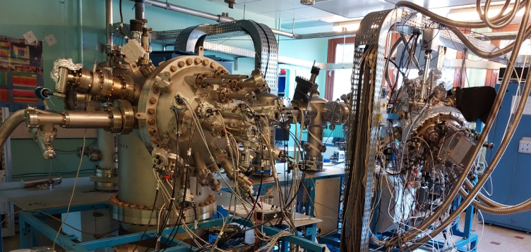
Molecular beam epitaxy (MBE) chambers (located at CEA, building C5)
Optical spectroscopy setups
Other expertise
NPSC has a long-standing expertise in the field of epitaxy of semiconductor materials and heterostructures. Our activities are of two kinds:
The team is equipped with an ensemble of six Molecular Beam Epitaxy chambers (MBE) and one Metal-Organic Chemical Vapour Deposition machine (MOCVD). They cover a wide range of materials (arsenides, tellurides, selenides, nitrides and oxides) and include two clusters (II-VI / arsenides / metals, and nitrides / oxides, connected under ultra-high vacuum for a better control of interfaces such as metals/ZnTe/InAs or AlN/Ga2O3). These materials are chosen for their greater interaction with light from IR to UV, for light emission, quantum optics and nano-photonics, or for their specific transport properties, from fundamental topological aspects to power electronics.
With our equipment and know-how, we use epitaxy to develop semiconductor objects of various dimensionalities (quantum dots, nanowires, quantum wells), materials in metastable phases and complex epitaxial interfaces between compounds who have no atoms in common, up to III-V / II-VI core-shell nanowires, nitride/oxide heterostructures, or metal-semiconductor interfaces.
The idea of single object and confinement is often central: an exciton in a quantum dot at the nanometer scale interacts with the spin of a single impurity, charge carriers (in a quantum dot) interact with photons in a microcavity or a photonic wire at the submicrometer scale for applications in quantum optics, the proximity effect between a semiconductor nanowire and a superconductor is controlled by an electrical bias or a tunnel barrier.
The epitaxy set-ups are run jointly by the CNRS, CEA and UGA staff. A significant part of the samples contributes to collaborations in France and abroad.
The cluster for oxides (left) and nitrides (right).
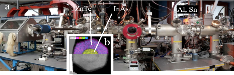
(a) the MBE cluster for II-VI / arsenides / metals; (b) cross-section of an InAs/ZnTe core/shell nanowire observed using transmission electron microscopy and energy-dispersive X-ray spectroscopy (courtesy Susheng Tan, Pittsburgh).
We are interested in controlling individual spins in semiconductors. Over the last few years, various systems based on diluted magnetic semiconductors have been studied: (i) Mn-doped quantum dots (QDs) with n-type codoping; and (ii) Cr-, Co- and Ni-doped QDs.
Regarding Mn, we have studied the triplet states of charged excitons interacting with the spin of magnetic atoms. Cr, Co and Ni are magnetic elements that are highly sensitive to strain and are considered promising for hybrid spin-mechanical systems. Intensive study of Cr-doped systems has led to: the observation of charge fluctuations in a single atom near a QD; the demonstration of the effect of optically generated non-equilibrium phonons on spin relaxation; and the observation of an additional stable oxidation state of Cr in a II-VI semiconductor: a Cr+ ion coupled to a hole spin (figure 1). This hole-Cr⁺ complex forms a nanomagnet that can be addressed using resonant optical excitation.
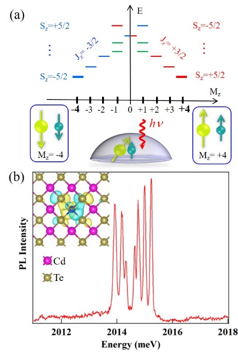
Figure 1: (a) Energy levels of the nanomagnet formed by the ferromagnetic coupling of the S=5/2 spin of Cr+ and the Jz=±3/2 spin of a heavy hole in a CdTe/ZnTe QD. (b) PL of a QD containing a hole-Cr+ nanomagnet. Circularly polarized excitation on the high-energy line allows the fundamental states Mz=+4 or Mz=-4 to be addressed. The inset shows a calculation of a Cr+ d orbital revealing hybridization with the Te orbitals. This hybridization is responsible for the exchange interaction with the hole spin.
In the case of Co²⁺, we demonstrated that coupling between two magnetic atoms in a QD can be induced by optical injection of spin-polarised carriers. For Ni²⁺, we have shown that its spin structure is strongly influenced by the orientation of the local strain tensor around the atom. We have also recently realized surface acoustic wave (SAW) devices in the GHz range on these non-piezoelectric II-VI magnetic systems, opening up the possibility of coherent mechanical control of individual spins.
Further reading:
Optical probing of the carriers-mediated coupling of the spin of two Co atoms in a quantum dot, L. Besombes, J. Kobak, W. Pacuski, Physical Review B 109, 235302 (2024).
Coupling of the triplet states of a negatively charged exciton in a quantum dot with the spin of a magnetic atom, L. Besombes, S. Ando, H. Boukari, S. Kuroda, Physical Review B 107, 235305 (2023).
Spin dynamics of positively charged excitons in Cr+ doped quantum dots probed by resonant photoluminescence, V. Tiwari, M. Morita, T. Inoue, S. Ando, H. Boukari, S. Kuroda, L. Besombes, Physical Review B 106, 045308 (2022).
A hole-Cr+ nano-magnet in a semiconductor quantum dots, Tiwari, M. Arino, S. Gupta, M. Morita, T. Inoue, D. Caliste, P. Pochet, H. Boukari, S. Kuroda, L. Besombes, Physical Review B 104, L0441301 (2021).
Radio frequency stress-induce modulation of CdTe/ZnTe quantum dots, V. Tiwari, K. Makita, M. Arino, M. Morita, S. Kuroda, H. Boukari, L. Besombes, Journal of Applied Physics 127, 234303 (2020).
Influence of non-equilibrium phonons on the spin dynamics of a single Cr atom, V. Tiwari, K. Makita, M. Arino, M. Morita, S. Kuroda, H. Boukari, L. Besombes, Physical Review B 101, 035305 (2020).
Charge fluctuations of a Cr atom probed in the optical spectra of a quantum dot, L. Besombes, H. Boukari, V. Tiwari, A. Lafuente-Sampietro, M. Sunaga, K. Makita, S. Kuroda, Physical Review B 99, 035309 (2019).
Optical nonlinearities usually appear for large intensities, but discrete transitions allow for giant nonlinearities operating at the single-photon level. We have demonstrated a two-mode giant nonlinearity with a single semiconductor quantum dot (QD) embedded in a photonic wire antenna. We have exploited two detuned optical transitions associated with the exciton-biexciton QD level scheme. Owing to the broadband waveguide antenna, the two transitions were efficiently interfaced with two free-space laser beams. We have shown [1] that the reflection of one laser beam can be controlled by the other beam, with a threshold power as low as 10 photons per exciton lifetime (1.6 nW). Such a two-color nonlinearity opens appealing perspectives for the realization of ultralow-power logical gates and optical quantum gates, and could also be implemented in an integrated photonic circuit based on planar waveguides.
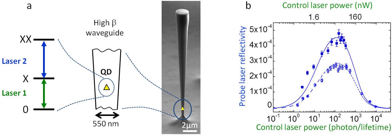
Fig.1: a, A single InAs QD embedded in a GaAs waveguide. The thre-level system is made of the excitonic (X) and the biexcitonic (XX) transitions.The β parameter is the fraction of light emitted by the QD that is guided by the wire. b, The probe (upper transition) reflectivity is displayed as a function of the control (lower transition) power for a probe power of 0.5 nW (solid squares) and 2.6 nW (empty circles).
References:
Hybrid quantum optomechanical systems offer an interface between a single two-level system and a macroscopical mechanical degree of freedom.
One of the major objectives for developing this concept is the realization of a quantum interface between a qubit and a mechanical oscillator with important technological applications for quantum information and ultra-sensitive measurements
We have built a hybrid system made of a vibrating microwire coupled to a single semiconductor quantum dot (QD) via material strain. We have shown a few years ago, that the QD excitonic transition energy can thus be modulated by the microwire motion [1] (cf Fig.2a,b). We have used this property to locate very precisely QD within the microwire [2] (cf Fig.2c).
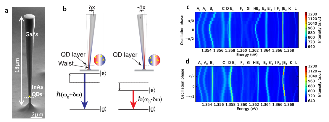
Fig. 2 a, Scanning electronic microscope image of the photonic wire. b, The strain field (color scale) induced by the wire oscillation shifts the quantum dot energy. c,d, Stroboscopic data showing the energy shift for different QDs as the wire oscillates along the X (Y) polarized mode in c (d).
Following a theoretical proposal [3], we have demonstrated the reverse effect whereby the wire is set in motion by the resonant drive of a single QD exciton with a laser modulated at the mechanical frequency [4] (Fig. 3). The resulting driving force is found to be almost 3 orders of magnitude larger than radiation pressure.
From a fundamental aspect, this state dependent force offers a convenient strategy to map the QD quantum state onto a mechanical degree of freedom.
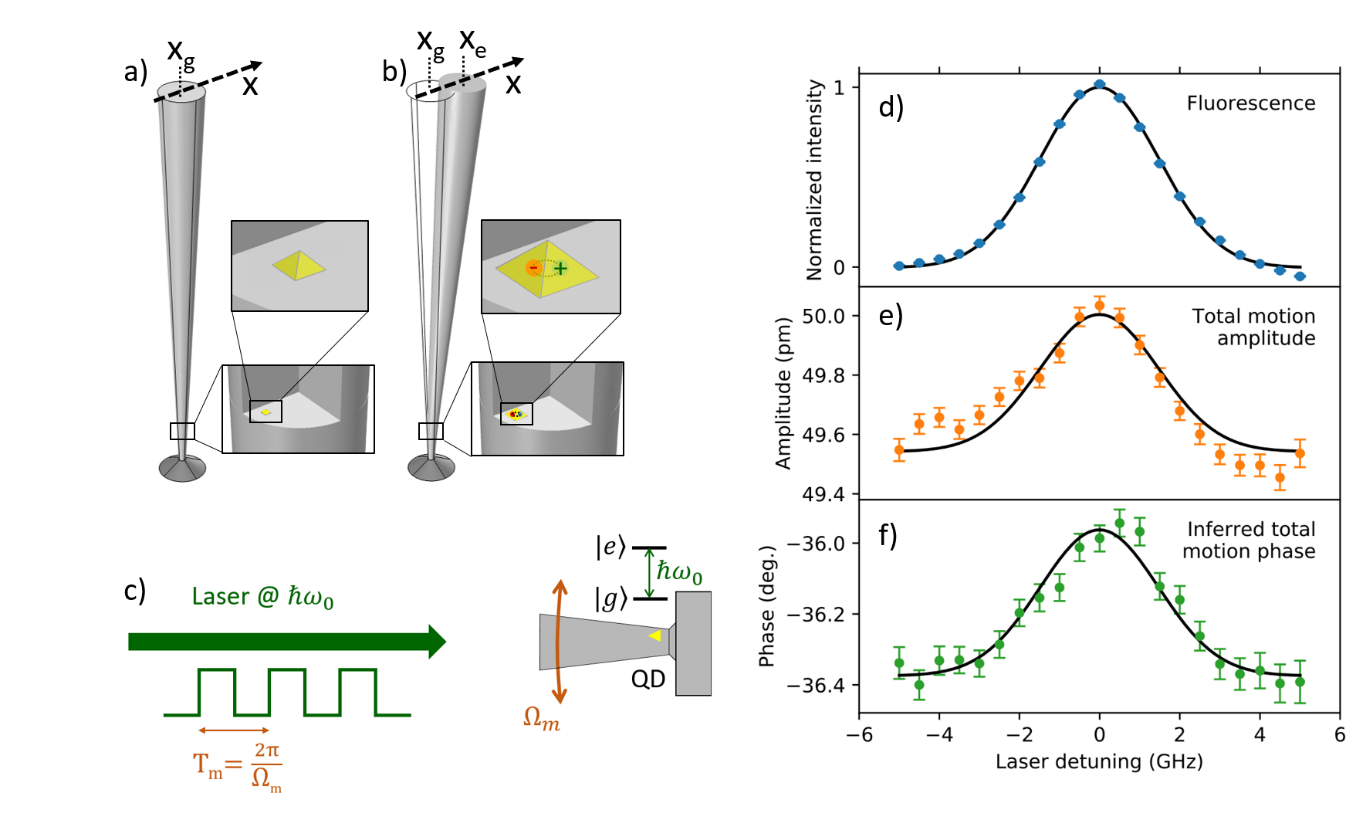
Fig. 3 a,b Schematic explanation of the effect. The lower insets are a cut of the wire showing the approximate position of the QD (yellow pyramid). When the QD is in its ground state (in a), the wire rest position is xg. When the QD is excited (hosts an exciton, represented as an orange electron and a green hole in b), its physical size is larger so that the rest position of the wire is displaced to xe. c, Principle of the experiment. The QD is illuminated by a laser resonant with its optical transition at ω0. The laser intensity is modulated at the wire mechanical frequency Ωm/2 and the wire motion is measured as a function of the laser detuning with respect to the QD transition. d, fluorescence light emitted by the QD as the laser is scanned across the QD resonance. Corresponding amplitude (e) and phase shift (f) of the wire motion, demonstrating the QD induced motion.
References:
We develop a new interpretation for quantum mechanics that is based on contextual objectivity and quantization. This leads, e.g., to original views on the origin of randomness and to the development of new concepts in quantum thermodynamics.
We establish a new research area on the study of quantum causality. Here the objective is to study the new types of causal relations that may exist in the quantum world. Indeed, quantum causal relations may have genuinely quantum features, and may be subject to similar quantum indefiniteness as quantum states: one can, e.g., find some “quantum superpositions of causal relations”. Along this line of research, we investigate a new framework that allows one to study quantum processes without imposing a well-defined causal structure; we clarify the concepts of interest and how to verify them in practice. We contribute to experimental demonstrations of such processes, and investigate their possible applications for quantum information processing.
A photonic implementation of the “quantum switch”: the polarisation ( |H> or |V> ) of a photon controls its trajectory through the above setup (via polarising beamsplitters, PBS, which transmit |H> and reflect |V>): a |H> photon first goes to A and then to B, and vice-versa for a |V> photon, where A and B are quantum operations applied to the state |Ψ> of another degree of freedom of the photon (e.g., the orbital angular momentum, as in the Brisbane experiment). A photon in a superposition |H>+|V> thus undergoes a superposition of the two orders AB and BA.
References:
We also investigate other aspects of the “quantum weirdness”, related in particular to the uncertainty principle, to the status of the wave function in quantum theory, to quantum entanglement and to quantum (or even post-quantum) nonlocality.
Regarding thermodynamics, we work on the energetic footprints of quantum noise and information. The essence of classical thermodynamics at the microscopic scale is to extract energy from hot baths and convert it into useful energy (work), turning thermal noise into a resource. Reciprocally, thermodynamics provides fundamental concepts to estimate the energetic cost of fighting against noise to maintain order. Since information is stored in physical systems, it also obeys the laws of thermodynamics.
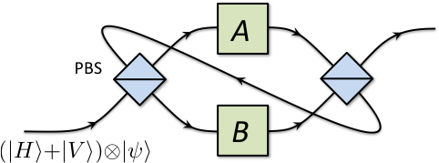
Our goal is to transpose the concepts and tools of (information) thermodynamics to the case where noise and information become quantum. On the one hand, this allows designing realistic nano-engines with no classical equivalent (e.g. coherence or quantum measurement driven engines, autonomous quantum Maxwell’s demons…) with clear quantum boosts and genuine quantum operating modes. The studies are conducted in collaboration with cutting edge experimentalists, on platforms with exquisite quantum control: semi-conducting quantum dots deterministically coupled to high Q cavities, superconducting circuits, Rydberg atoms. A complementary axis consists in bridging the gap between optomechanical systems and quantum thermodynamics, owing to the potential of these systems for direct measurement of work exchanges.
Schema of a quantum Maxwell’s-daemon experiment. The qubit states (|g>, |e>) and a driving field exchange work with each other, while it is being periodically measured by the daemon in the {|+x>, |-x>} basis. Each time the daemon measures |-x>, it performs a feedback on the qubit to bring it into the state |+x>, the state which is favourable for extracting work from the qubit.
References:
We have used optical spectroscopy and four-wave mixing (FWM) [1] to investigate fundamental electronic properties of 2D materials. Ongoing research focuses on well-studied 2D Transition Metal Dichalcogenides (TMDs) and 2D halide perovskites.
Both materials are prototypical 2D materials with excitons that feature strict quantum confinement in monolayers, characterized by binding energies and oscillator strengths that are orders of magnitude greater than those in standard semiconductors, such as GaAs or CdTe. Their fundamental electronic states, however, are compact tightly bound excitons in 2D TMDs, and spatially extended exciton polaritons (mixed exciton-photon quasi-particles; see Figure A) in 2D halide perovskites, even in layers as thin as 30 nm [2].
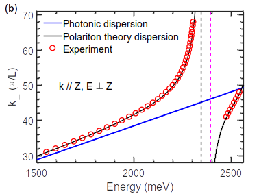
Evidence of exciton polariton in 2D halide perovskite. Open red dots: Energy dispersion of Fabry-Perot-like modes observed in Reflectance spectrum of a L = 6.6 μm thick layer of (C6H5C2H4NH3)2PbI4 for incident photons with wave vector k//z and electric field E ⊥ z (z axis being perpendicular to 2D (x, y) plane). Solid black curves: Simulation assuming 2D halide perovskite layer as a dielectric layer with complex Lorentz permittivity. Separation between vertical dashed lines = Longitudinal-transverse exciton splitting.
Even though the linear optical response of 2D TMDs is often dominated by disorder-induced broadening, we have shown that FWM spectroscopy is well-suited to extract the homogeneous and inhomogeneous contributions to this broadening [3, 4] or to evaluate the impact of free carriers on coherent couplings [4].
Thus, one expects markedly different temporal and spatial coherence in the 2D perovskites since sensitivity to local potential fluctuations and lattice vibrations scales inversely with extension of quasi-particle wavefunctions.
We also currently explore coherence dynamics in novel 2D materials, specifically CrSBr and moiré superlattices of TMD bilayers with tunable twist angles.
[1] Daniel Groll, Thilo Hahn, Paweł Machnikowski, Tilmann Kuhn, Jacek Kasprzak and Daniel Wigger. « Fundamentals of heterodyne wave mixing spectroscopy: a tutorial », Nano Futures 9, 042601 (2025).
[2] Le Khanh Linh, Le Si Dang, Nguyen Tran Thuat, Regis André, Joël Cibert, David Ferrand. « Anisotropic excitons in caste-capping 2D perovskites with vertical and horizontal orientations », International Conference on Optics of Excitons in Confined Systems (OECS19), 14th to 18th July 2025, Warsaw, Poland.
[3] Karolina Ewa Połczyńska, Simon Le Denmat, Takashi Taniguchi, Kenji Watanabe, Marek Potemski, Piotr Kossacki, Wojciech Pacuski and Jacek Kasprzak. « Coherent imaging and dynamics of excitons in MoSe₂ monolayers epitaxially grown on hexagonal boron nitride », Nanoscale 15, 6941-6946 (2023).
[4] Caroline Boule, Diana Vaclavkova, Miroslav Bartos, Karol Nogajewski, Lukas Zdrazil, Takashi Taniguchi, Kenji Watanabe, Marek Potemski and Jacek Kasprzak. « Coherent dynamics and mapping of excitons in single layer MoSe₂ and WSe₂ at the homogeneous limit », Physical Review Materials 4, 034001 (2020).
[5] Aleksander Rodek, Thilo Hahn, James Howarth, Takashi Taniguchi, Kenji Watanabe, Marek Potemski, Piotr Kossacki, Daniel Wigger and Jacek Kasprzak. « Controlled coherent-coupling and dynamics of exciton complexes in a MoSe2 monolayer », 2D Materials 10, 025027 (2023).
Contacts: David Ferrand and Jacek Kasprzak
In the team, we develop nanowires based on GaAs and InAs semiconductors. InAs and GaAs can be combined in heterostructures to form quantum dots. We use those quantum dots for single photon emission applications.
Our InAs nanowires are also combined with superconductors to form core shell heterostructures. They are integrated into quantum devices such as gatemon quantum bits or into devices designed to search for exotic particles that live in topological superconductors.
Semiconductor Quantum dots (QDs) have become the gold standard for on-demand single-photons, a cornerstone of quantum optics and communication. While most of the efforts are devoted to single photon emission in the so-called telecom band (1.5 μm) or in the near infrared, there is a growing demand for shorter wavelengths, in particular the blue-green range for free-space and underwater communication. We fabricate by molecular beam epitaxy (see Research activities / Epitaxy of semiconductors) CdSe QDs embedded in ZnSe nanowires, with typical dimensions as shown in the figure. They emit at 0.5 μm. The nanowire geometry allows us to obtain a high brightness (12 MHz repetition rate). Single photon emission is observed up to room temperature while keeping a good purity (ability to emit one and only one photon per pulse) [1].
We presently explore the effects of charges and temperature on the characteristics of the single-photon emission. It led us to the development of a local thermometry procedure based on the analysis of the shape of the spectral line [2]. Other developments aim at exploiting the specificities of the growth of II-VI nanowires (it is seeded by a crystallized gold nanoparticle [3], not by a liquid droplet) in order to achieve a pre-determined, site-selective growth. A goal is to insert the emitter into a photonic circuit or an electronic structure.
Left: Scanning electron microscopy image of a ZnSe nanowire containing a CdSe quantum dot; Right bottom: superimposed SEM image, and cathodoluminescence image at the wavelength of the quantum dot; Right top: electron energy dispersive spectroscopy image of a CdSe quantum dot.
[1] Brightness and purity of a room-temperature single-photon source in the blue-green range, Francis Granger, Saransh Raj Gosain , Gilles Nogues, Edith Bellet-Amalric, Joël Cibert, David Ferrand, and Kuntheak Kheng, hal-04034474, Optics Letters 48, 3833 (2023).
[2] Calibration-free measurement of the phonon temperature around a single emitter, Francis Granger, Edith Bellet-Amalric, Kuntheak Kheng, Gilles Nogues, David Ferrand, Joël Cibert, hal-04957849, ACS Nano 19, 20914 (2025).
[3] Regulated Dynamics with Two-Monolayer Steps in Vapor-Solid-Solid Growth of Nanowires, Edith Bellet-Amalric, Federico Panciera, Gilles Patriarche, Laurent Travers, Martien Den Hertog, Jean-Christophe Harmand, Frank Glas, Joël Cibert, hal-03475082, ACS Nano 16, 4397 (2022).
In addition to semiconductors, the NPSC team also studies the remarkable optical properties of studies rare earth ions embedded into crystals. These properties offer an ideal platform for several applications in quantum technologies, mainly quantum memories and RF-to-optical photon transducers. Our expertise is based on in-depth knowledge of materials and the limits of coherence in these systems. We are also committed to developing our instruments, particularly for low-temperature optics. Highly doped rare-earth crystal are also the best system so far to observe solid state optical cooling. We study this phenomenon in collaboration with Air Liquide to assess its potential for spatial cryocoolers.
We mainly work with erbium as a rare earth dopant, as it has the advantage of having an optical transition that is directly compatible with the fibre optic telecommunications network.
In the field of quantum memories, current efforts are focused on integrating active materials with photonic structures.
We are currently working on integrating yttrium oxide onto a glass substrate to form a 2D slab waveguide that will serve as the basis for the subsequent manufacturing of 1D waveguides and resonant photonic structures [Projet QMEMO].
Thin Y2SiO5 crystal (10um) bonded to a glass substrate (left: profilometer depth scan, right: optical image).
A recent effort has been made to consider the insertion of erbium directly into silicon. The characterisation of the dopant is particularly encouraging for applications [Holzäpfel 2025]
RF-to-optical photon transducers serve to link superconducting or spin qubits to fibre telecommunication networks. They coherently convert optical and RF fields at the single photon level. Erbium is doubly relevant for this application: in addition to its telecom transition, it has an electron spin whose frequency is compatible with superconducting qubits. The coupling scheme is therefore doubly resonant, in the sense that the optical and spin transitions are directly excited with enhanced efficiency.
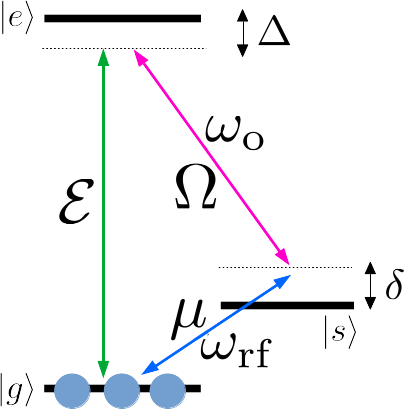
Doubly resonant level scheme. A strong optical field (magenta) is applied in a lambda system, where the optical (green) and RF (blue) signals are resonant with the other branches
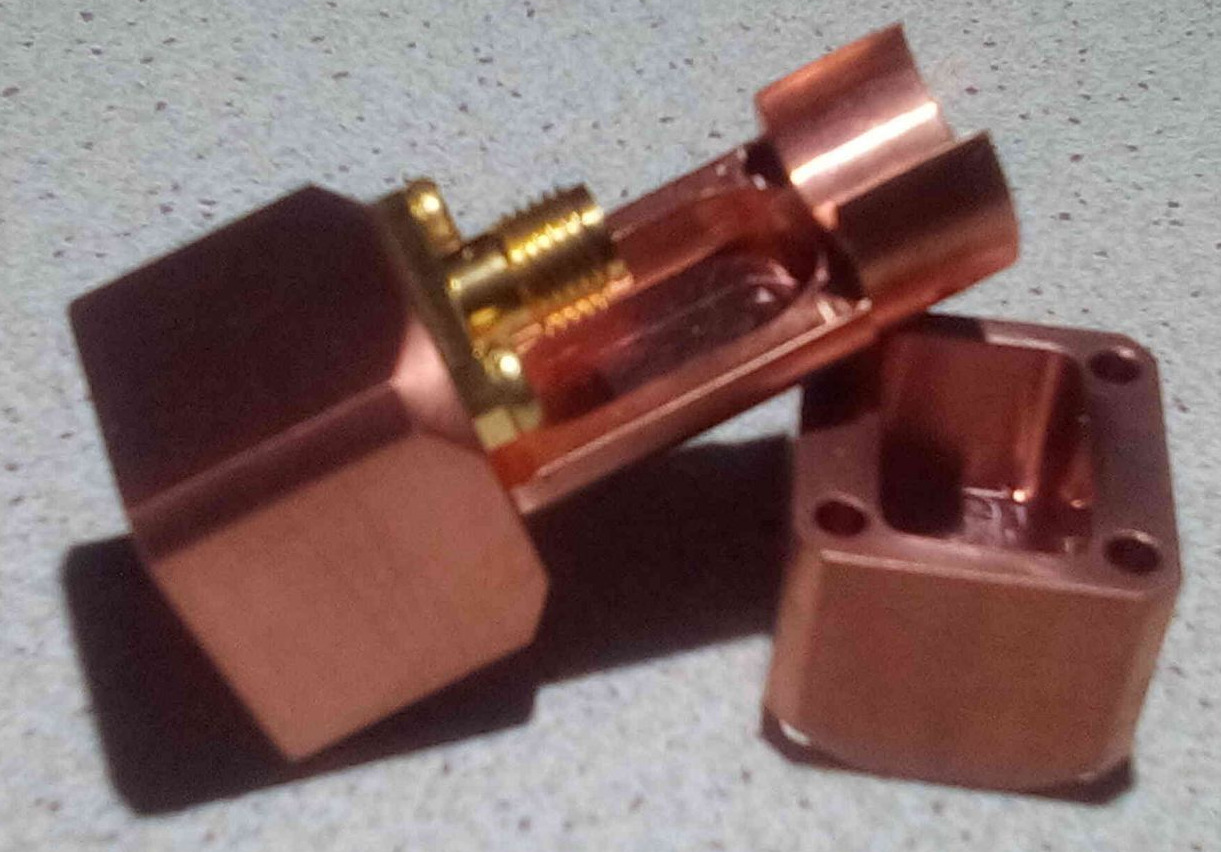
3D rectangular RF cavity (copper) resonant with the erbium spins at 12GHz with optical access (tiny holes)
Further reading:
Contact: Thierry Chanelière
We are also studying the strain effect on optical transitions. Although rare earths are not very sensitive to constraints in terms of absolute value, the sharpness of the transitions makes the effect particularly visible. We are specifically interested in the so-called back-action, when resonant optical excitation produces local distortions.
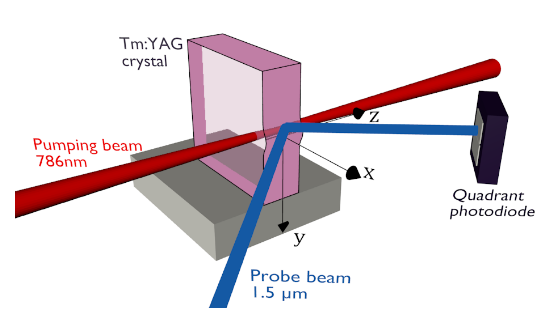
Photodeflection setup to measure optomechanical back-action when thulium ions are resonantly excited
Further reading:
Contacts: Thierry Chanelière, Jean-Philippe Poizat
We are working to improve the coherence properties of rare earth-doped materials in different crystalline matrices. Our expertise is based on microscopic knowledge of the active ion insertion site (crystal field analysis) and on modeling interactions with surrounding ions.
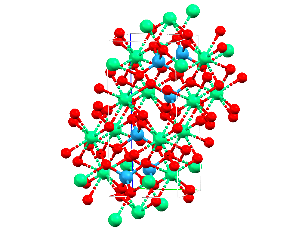
Unit cell of CaWO4 in which Er substitutes Ca ion (in blue). We here model the action of applied strain on the crystal field.
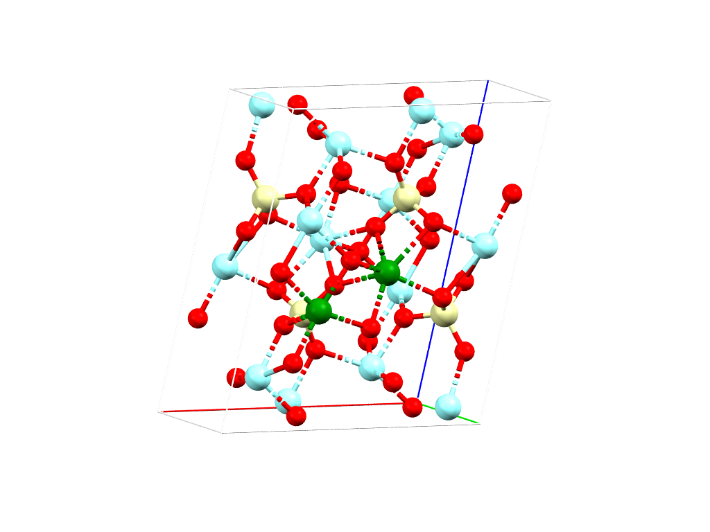
Unit cell of Y2SiO5. The two possible sites of erbium are represented in dark green. The dominant dipolar interaction occurs with the surrounding yttrium ions (light blue)
Further reading:
Contact: Thierry Chanelière
We are also working on the instrumental developments necessary for the implementation of low-temperature optical technologies.
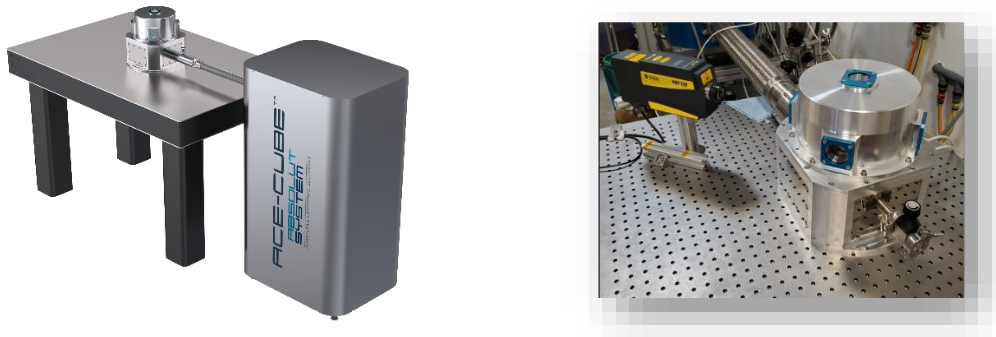
The ACE-CUBE cryogenic platform produced by Absolut System in collaboration with the Institut Néel.
Further reading:
Optical cooling is a phenomenon where a crystal emits more optical power than it absorbs, leading to its cooling. In collaboration with Air Liquide Advanced Technologies (AL-AT, Sassenage), we are studying its potential for a new kind of space cryocooler embedded in a satellite. It will pave the way to contact-less, vibration-free cooling of sensitive equipments down to about 100 K. To test this possibility, researchers and technical staff of Institut Néel have built and successfully operated a first prototype of a fiber-coupled lasercooler.
The principles of optical cooling derive from the very first studies on the interaction of light with matter. In 1852 Stokes explains the phenomenon of fluorescence and observes that in some materials the wavelength of the emitted light is different from the one of the absorbed light. Most interestingly, this ‘Stokes shift’ can be negative, re-emitting light with a shorter wavelength. This observation lead Pringsheim to assert in 1929 that repeated cycles of absorption and fluorescence (with a higher-energy photon) extract energy from the material, hence leading to its cooling. The first clear experimental demonstration of cooling took place in 1995 after progresses in lasers and in growth science that allowed producing good enough materials. Indeed, cooling happens if and only if each absorption event is followed by a fluorescent photon escaping the crystal. Any other phenomenon leads to a net heating two orders of magnitude larger than the cooling process! Colleagues from the University of Pisa provided a Yb3+ doped YLiF4 crystal (Yb:YLF), which is the best material for laser cooling so far.
Laser cooling is considered by ALAT as a potential breakthrough technology in the market of space cryocoolers which are required for infra-red detectors in Earth-observation missions. It offers many advantages over existing solutions based on pulsed-tube coolers: no vibrations, solid-state cooling with no moving parts, no electromagnetic perturbation and a dramatic reduction of volume. Preliminary studies comparing the requirements of a laser cooler and a pulsed-tube cooler in terms of size, weight and power for an earth-observation satellite show that in spite of a significantly higher use of power, a laser cooler requires less volume and up to 20% less weight.
A practicable implementation of a laser cooler requires separating the cooling head from the laser source. We designed an original setup where a high-power single mode polarization maintaining fiber connects the two systems. In order to minimize the thermal load on the crystal, the setup is pumped to reduce convection, the crystal stands on low-conduction silica aerogel pads and is mounted inside a ‘clamshell’ whose surfaces are coated by a low-emissivity Tinox layer in order to reduce radiative transfers and efficiently absorb the crystal fluorescence. The experimental setup was designed with the support of the Experimental Engineering technical group, which also machined and assembled its inner core.
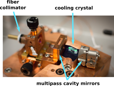
Photograph of the laser cooling experimental bench. The Yb:YLF crystal sits on 2 silica aerogel pads. The laser power is coupled through a fiber collimator inside a multipass cavity to be fully absorbed in the crystal. The green light in the crystal comes from the fluorescence of Er impurities.
Contact-free thermometers are used to monitor the crystal temperature. First a carefully calibrated thermal camera is used, down to a temperature of 160 K. Below this limit, a fluorescence spectroscopy method is used, which allowed us to record a minimum temperature of 125K for 11 W of absorbed power. After the laser is switched off, the return to equilibrium at room temperature allows evaluating the conductive and radiative thermal loads on the crystal and hence the cooling power, which is in good agreement with a simple model.
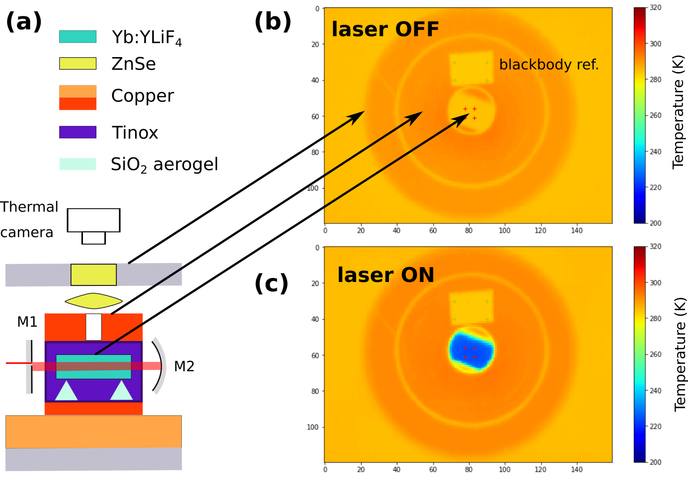
(a) cut of the experiment. A set of ZnSe optics allows recording its image on a thermal camera. (b) Thermal image with no cooling laser. The different temperature readings are due to the different emissivities of the materials and finite transmission of the lenses. (c) Same image when the cooling system is on.
Our collaboration with ALAT continues. It now concerns the thermal link between the cooling crystal and the object that is to be cooled. This task is addressed in collaboration with the Massive Crystals technological platform of Institut Néel. The link will be made of MgF2, cut, oriented and polished by the platform and attached to the crystal by optical adhesion. Another objective is to design a compact cooling experiment.
Further readings:
Contact: Gilles Nogues
2024 post-doc – BUATIP Natthawadi
2024 post-doc – KOTEVA Konstantina
2024 post-doc – FREROT Iréné
2024 thèse – PRASAD Samyak
2024 thèse – MOTHE Raphael
2023 post-doc – PICCIONE Nicolo
2023 thèse – GAIGNARD Maxime
2023 thèse – GOES Bruno
2023 post-doc – MAFFEI Maria
2022 thèse – BRESQUE Léa
2022 post-doc – WEIN Stephen
2022 post-doc – NAHRA Mackrine
2022 thèse – CHEN An-Hsi
2022 post-doc – DARDAILLON Rémi
2022 thèse – LAZOURENKO-DOURDENT Hippolyte
2022 thèse – LETERTRE Laurie
2021 thèse – FELLOUS-ASIANI Marco
2021 thèse – VINCENTE Rémi
2021 thèse – TIWARI Vivekanand
2021 thèse – KLOSS Enzo
2020 post-doc – CAMATI Patrice
2020 post-doc – MARIANI Cristian
2020 thèse – WECHS Julian
2019 thèse – MONSEL Juliette
2019 thèse – MORATIS Kimon
2019 thèse – VAISH Nitika
2019 thèse – JALOUSTRE Lucas
2018 thèse – REZNYCHENKO Bogdan
2018 post-doc – ABBOTT Alastair
2018 post-doc – KETTLER jan
2018 thèse – LAFUENTE-SAMPIETRO Alban
2018 thèse – BEZNASYUK Daria
2017 thèse – ELOUARD Cyril
2017 thèse – DELMONTE Valentin
2017 post-doc – JAKUBCZYK Tomasz
2017 post-doc – DE-ASSIS Pierre-Louis
2017 thèse – TUMANOV Dmitrii
2017 thèse – ORRU Marta
2016 thèse – JEANNIN Mathieu
2016 post-doc – TAN Siew-li
2016 thèse – NGUYEN Hoai-anh
2016 post-doc – FERRARI Alberto
2016 thèse – ARTIOLI Alberto
2015 post-doc – GRANGE Thomas
2015 post-doc – VACANTI Giovani
2015 thèse – MERMILLOD Quentin
2015 post-doc – KLEMBT Sebastian
2015 thèse – RUEDA-FONSECA Pamela
2013 thèse – ELOUNEG-JAMROZ Myriam
2013 thèse – GERARD Lionel
2013 thèse – STEPANOV Petr
2012 thèse – BOUNOUAR Samir
2012 thèse – CAO Chong long
2012 thèse – DINIZ Igor
2012 thèse – TRICHET Aurélien
2012 thèse – VALENTE Daniele
2012 thèse – YEO Inah
2012 post-doc – BRUNETTI Adalberto
2012 post-doc – FRAS François
2012 post-doc – MEDARD François
2011 thèse – LE GALL Claire
2011 post-doc – PORTOLAN Stephano
2010 thèse – YU Ing-Song
2010 post-doc – WOJNAR Piotr
2010 post-doc – KOLODKA Roman
2009 thèse – CLEMENT Thomas
2009 thèse – MUNSCH Mathieu
2009 thèse – SALLEN Gregory
2008 thèse – NAJJAR Rita
Position type: Stages Master-2 & Thèse
Contact: Thierry Chanelière - 04 76 88 10 07
We propose to control the erbium emission in SOI (Silicon On Insulator) using acoustic waves, offering a new control knob of quantum memories transitions. This approach takes full advantage of the confinement due to the nanometric size of the Si layer and well-established techniques for depositing piezoelectric pads.
Position type: Stages Master-2 & Thèse
Contact: Besombes Lucien - 04 56 38 71 58
This internship aims to study optically and model the dynamics of the coupled electronic and nuclear spins of an individual vanadium atom embedded in an optically active semiconductor quantum dot.
Position type: Stages Master-2 & Thèse
Contact: SONGMUANG Rudeesun -
In recent decades, there has been significant progress in biomedical devices that can be implanted in the human body for diagnostic and treatment purposes. However, most of them rely on batteries presenting a challenge for miniaturization and extending their operational lifespan. Recent advancements in piezoelectric energy harvesters (PEHs) offer a solution by enabling the realization of self-sustainable devices, which can convert mechanical energy from human movements directly into electricity. Yet, traditional rigid energy conversion systems are unsuitable for such applications due to their incompatibility with soft tissue and curved surfaces, encouraging the development of flexible, and lightweight PEHs.
Person in charge: Lucien BESOMBES, Edith BELLET-AMALRIC
Permanents
Students & Post-docs & CDD
Lucien BESOMBES
Personnel Chercheur - CNRS
lucien.besombes [at] neel.cnrs.fr
Phone: 04 56 38 71 58
Office: C3-201
Cyril BRANCIARD
Personnel Chercheur - CNRS
cyril.branciard [at] neel.cnrs.fr
Phone: 04 56 38 70 60
Office: C3-212
Jesus CANAS
Personnel Chercheur - CNRS
jesus.canas [at] neel.cnrs.fr
Phone: 04 76 88 74 64
Office: CEA-C5-670
Thierry CHANELIERE
Personnel Chercheur - CNRS
thierry.chaneliere [at] neel.cnrs.fr
Phone: 07 76 88 10 07
Office: C3-201
Joël CIBERT
Personnel Chercheur - CNRS
Joel.Cibert [at] neel.cnrs.fr
Phone: 04 76 88 11 93
Office: C3-200
Lorenzo DE-SANTIS
Personnel Chercheur - CNRS
lorenzo.de-santis [at] neel.cnrs.fr
Phone: 04 76 88 90 77
Office: C3-211
David FERRAND
Personnel Chercheur - UGA
david.ferrand [at] neel.cnrs.fr
Phone: 04 56 38 70 45
Office: C3-200
Moïra HOCEVAR
Personnel Chercheur - CNRS
moira.hocevar [at] neel.cnrs.fr
Phone: 35 13
Office: CEA-C5-628
Jacek KASPRZAK
Personnel Chercheur - CNRS
jacek.kasprzak [at] neel.cnrs.fr
Phone: 04 56 38 71 64
Office: C3-212
Pierre LEMONDE
Personnel Chercheur - CNRS
pierre.lemonde [at] neel.cnrs.fr
Phone: 04 76 88 10 90
Office: C3-211
Henri MARIETTE
Personnel Chercheur - CNRS
henri.mariette [at] neel.cnrs.fr
Phone: 56 88
Office: CEA-C5-683
Gilles NOGUES
Personnel Chercheur - CNRS
gilles.nogues [at] neel.cnrs.fr
Phone: 04 56 38 71 64
Office: C3-212
Jean-Philippe POIZAT
Personnel Chercheur - CNRS
jean-philippe.poizat [at] neel.cnrs.fr
Phone: 04 56 38 71 65
Office: F-405
Rudeesun SONGMUANG
Personnel Chercheur - CNRS
rudeesun.songmuang [at] neel.cnrs.fr
Phone: 04 76 88 10 44
Office: F-212
Shashank ARUNKUMAR
Personnel Chercheur - CNRS
shashank.arunkumar [at] neel.cnrs.fr
Phone: 04 76 88 11 40
Office: F-209
Referent: Gilles NOGUES
Antonin CARON
Personnel Technique - CNRS
antonin.caron [at] neel.cnrs.fr
Phone: 04 76 88 11 40
Office: F-209
Referent: Jacek KASPRZAK
Emilien DE-BANK
Personnel Chercheur - UGA
emilien.de-bank [at] neel.cnrs.fr
Referent: Cyril BRANCIARD
Amanda-Maria FONSECA
Personnel Chercheur - UGA
amanda-maria.fonseca [at] neel.cnrs.fr
Referent: Cyril BRANCIARD
Mahnoor HANAN
Personnel Chercheur - CNRS
mahnoor.hanan [at] neel.cnrs.fr
Phone: 04 76 88 10 44
Office: F-212
Referent: Rudeesun SONGMUANG
Kim JUNGWON
Personnel Chercheur - CNRS
kim.jungwon [at] neel.cnrs.fr
Phone: 04 56 38 70 11
Office: F-208
Referent: Jacek KASPRZAK
Ved KUNTE
Personnel Chercheur - UGA
ved.kunte [at] neel.cnrs.fr
Phone: 04 76 88 78 13
Office: F-422
Referent: Cyril BRANCIARD
Abdessamad OUKERMOU
Personnel Technique - CNRS
abdessamad.oukermou [at] neel.cnrs.fr
Phone: 04 76 88 74 05
Office: F-205
Referent: Thierry CHANELIERE
Benjamin VIOLLET
Personnel Chercheur - UGA
benjamin.viollet [at] neel.cnrs.fr
Office: CEA-X
Referent: Moïra HOCEVAR
Shijun ZHANG
Personnel Chercheur - UGA
shijun.zhang [at] neel.cnrs.fr
Phone: 04 76 88 74 05
Office: F-205
Referent: Thierry CHANELIERE
Rakia ZOUAOUI
Personnel Chercheur - CNRS
rakia.zouaoui [at] neel.cnrs.fr
Office: F-323
Referent: Moïra HOCEVAR
Juan-Esteban ZURITA-LEMA
Personnel Chercheur - CNRS
juan-esteban.zurita-lema [at] neel.cnrs.fr
Office: CEA-X
Referent: Jesus CANAS
Edith BELLET-AMALRIC
Personnel Chercheur - CEA
edith.bellet-amalric [at] neel.cnrs.fr
Phone: 46 04
Office: CEA-C5-528
Julien CLAUDON
Personnel Chercheur - CEA/INAC
julien.claudon [at] cea.fr
Phone: 49 84
Office: CEA-C5-627
Ettore COCCATO
Personnel Chercheur - CEA
ettore.coccato [at] neel.cnrs.fr
Office: CEA-X
Referent: Eva MONROY
Laure COUDRAT
Personnel Chercheur - CEA
laure.coudrat [at] neel.cnrs.fr
Office: CEA-X
Referent: Regis ANDRE
Christophe DURAND
Personnel Chercheur - UGA
christophe.durand [at] cea.fr
Phone: 19 77
Office: CEA-C5-676
Maxime GAIGNARD
Personnel Chercheur - CEA
maxime.gaignard [at] cea.fr
Office: CEA-X
Referent: Jean-Philippe POIZAT
Jean-Michel GERARD
Personnel Chercheur - CEA/INAC
jean-michel.gerard [at] cea.fr
Phone: 31 34
Office: CEA-C5-664
Kuntheak KHENG
Personnel Chercheur - CEA
kuntheak.kheng [at] neel.cnrs.fr
Phone: 47 01
Office: CEA-C5-613
Hajer TLILI
Personnel Chercheur - UGA
hajer.tlili [at] neel.cnrs.fr
Phone: 04 56 38 70 85
Office: Z-206
Referent: Julien CLAUDON
Laura-Daniela VALLEJO-MELGAREJO
Personnel Chercheur - UGA
laura-daniela.vallejo-melgarejo [at] neel.cnrs.fr
Office: CEA-X
Referent: Edith BELLET-AMALRIC