- Accueil
- Institut Néel
- Équipes de recherche
- Pôles & Services techniques
- Travailler à l’institut
- Partenariats
- Actualités
- Agenda
- Annuaire
Nanofab est à la fois une centrale de proximité, reconnue par le Ministère de la Recherche et un pôle technologique de l’Institut Néel.
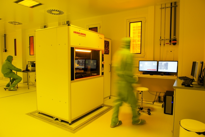
©CNRSPhototheque-CyrilFRESILLON
La Plateforme Nanofab est totalement insérée dans un laboratoire de recherche, très ouverte aux autres laboratoires (CEA, CNRS, UGA, G-INP) dans son fonctionnement et destinée à la réalisation d’objets nanométriques, souvent uniques en utilisant un nombre limité d’étapes lithographiques. Les demandes des équipes de recherches, issues ou non du monde « nano » sont souvent très « exotiques » en termes de besoins technologiques. Nanofab est ainsi souvent amené a développer des solutions techniques originales, parfois spécifiques à un échantillon, et aussi parfois à orienter ces projets vers d’autres centrales plus compétentes dans le domaine.
La salle blanche accueille chercheurs et étudiants de l’Institut Néel et des Laboratoires voisins. Thésards, post-docs et stagiaires sont formés aux techniques de nanofabrication. Des Travaux Pratiques sont organisés à destination des étudiants de l’UGA ( TP Cesire) ou de l’ESONN.
La salle blanche a une superficie de 220 m2. Elle est installée dans le nouveau Bâtiment Nanosciences de l’Institut Neel inauguré en 2013.
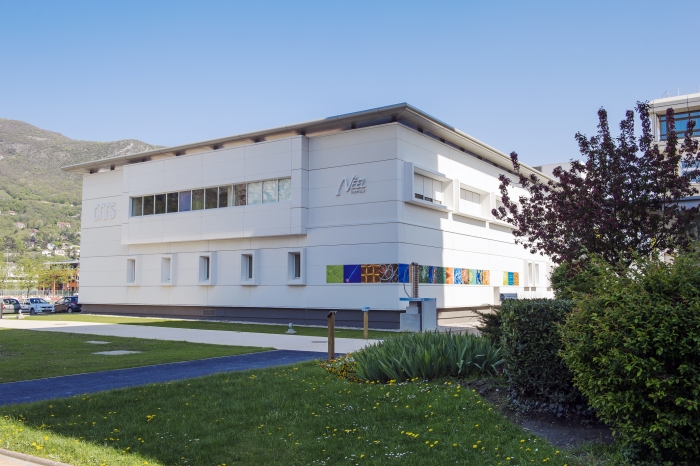
Bâtiment Z ©CNRSPhototheque-CyrilFRESILLON
![]()