- Accueil
- Institut Néel
- Équipes de recherche
- Pôles & Services techniques
- Travailler à l’institut
- Partenariats
- Actualités
- Agenda
- Annuaire
Our research group focuses on a family of semiconductors called wide bandgap (GaN and ZnO) and ultra-wide bandgap (diamond, AlN and Ga2O3). The driving force is the development of innovative electronic devices based on these materials for power electronics, light emitting devices and sensors. For this purpose, our activities include fundamental studies such as heterostructures, electron or exciton transport in nanowires, impurity centres or electron-phonon coupling and superconductivity, as well as the technological developments necessary for the fabrication of devices with tailored electronic properties, such as epitaxial growth with in-situ control, nanofabrication, impurity incorporation and gate oxide deposition.
Diamond device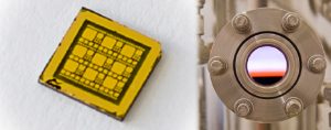
Plasma image during plasma enhanced chemical vapor deposition diamond growth
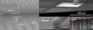
Ensemble of AlN nanowires pn junction: contact and electrical measurement
Person in charge: David EON
Students & Post-docs & CDD
Invited & Others
David EON
Personnel Chercheur - G-INP
david.eon [at] neel.cnrs.fr
Office: D-312
Philippe FERRANDIS
Personnel Chercheur - UGA
philippe.ferrandis [at] neel.cnrs.fr
Phone: 04 76 88 74 64
Office: D-417
Etienne GHEERAERT
Personnel Chercheur - G-INP
Etienne.Gheeraert [at] neel.cnrs.fr
Phone: 04 56 38 70 84
Office: D-309
Gwénolé JACOPIN
Personnel Chercheur - CNRS
gwenole.jacopin [at] neel.cnrs.fr
Phone: 04 76 88 11 83
Office: D-312
Julien PERNOT
Personnel Chercheur - UGA
Julien.Pernot [at] neel.cnrs.fr
Phone: 04 56 38 70 83
Office: D-309
Victor DINIEL
Personnel Chercheur - CNRS
victor.diniel [at] neel.cnrs.fr
Phone: 04 76 88 74 72
Office: D-315
Referent: David EON
Nicolas GUILLAUME
Personnel Chercheur - UGA
nicolas.guillaume [at] neel.cnrs.fr
Phone: 04 76 88 74 69
Office: D-423
Referent: Philippe FERRANDIS
Halilou ILBOUDO
Personnel Chercheur - CNRS
halilou.ilboudo [at] neel.cnrs.fr
Phone: 04 76 88 70 61
Office: D-318
Referent: Julien PERNOT
Francesco LA-ROCCA
Personnel Chercheur - CNRS
francesco.la-rocca [at] neel.cnrs.fr
Phone: 04 76 88 70 61
Office: D-318
Referent: Gwénolé JACOPIN
Leonardo LAGHEZZA
Personnel Technique - CNRS
leonardo.laghezza [at] neel.cnrs.fr
Phone: 04 76 88 70 61
Office: D-318
Referent: Julien PERNOT
Gabriel MESAS-PENA
Personnel Chercheur - Université de Cadiz
gabriel.mesas-pena [at] neel.cnrs.fr
Referent: Julien PERNOT
Marine REGNIER
Personnel Chercheur - CNRS
marine.regnier [at] neel.cnrs.fr
Phone: 04 76 88 74 69
Office: D-423
Referent: Etienne GHEERAERT
Alvaro REVILLA-MARTIN
Personnel Chercheur - UGA
alvaro.revilla-martin [at] neel.cnrs.fr
Phone: 04 76 88 74 69
Office: D-423
Referent: Julien PERNOT
Hugo RIBEIRO
Personnel Chercheur - CNRS
hugo.ribeiro [at] neel.cnrs.fr
Phone: 04 76 88 70 61
Office: D-318
Referent: Gwénolé JACOPIN
Juan-Carlos TRUJILLO-YAGUE
Personnel Chercheur - CNRS
juan-carlos.trujillo-yague [at] neel.cnrs.fr
Phone: 04 76 88 74 69
Office: D-423
Referent: Philippe FERRANDIS
Sakura UEHARA
Personnel Chercheur - Université d'Hokkaido - Japon
sakura.uehara [at] neel.cnrs.fr
Referent: Julien PERNOT
Marielena VELASCO ENRIQUEZ
Personnel Chercheur - UGA
marielena.velasco-enriquez [at] neel.cnrs.fr
Phone: 04 76 88 74 69
Office: D-423
Referent: Philippe FERRANDIS
Corentin GUERIN
Personnel Chercheur - CEA
corentin.guerin [at] neel.cnrs.fr
Office: CEA-X
Referent: Gwénolé JACOPIN