- Accueil
- Institut Néel
- Équipes de recherche
- Pôles & Services techniques
- Travailler à l’institut
- Partenariats
- Actualités
- Agenda
- Annuaire
The QuNES research fields embrace mesoscopic physics, quantum nano-electronics, and surface science. The main topics are electronic properties of 2D materials such as graphene and transition metal dichalcogenides, topological orders in Dirac materials, quantum thermodynamics, hybrid superconducting devices, many-body physics in semiconductor quantum dots and point contacts, and strongly disordered superconductors. The originality of the QuNES team is to combine quantum transport measurements with local probe measurements, using scanning tunneling microscopy and spectroscopy, atomic force microscopy, and scanning gate microscopy, at very low temperature, in ultra high vacuum, and under high magnetic fields.
|
|
Electronic properties of 2D materials |
|
|
Topological phases in Dirac materials |
|
|
Team S2D |
|
|
Thermodynamics of quantum devices |
|
|
Kondo cloud extension around quantum dots |
|
|
Strongly disordered superconductors |
Pierre Mallet, Jean-Yves Veuillen
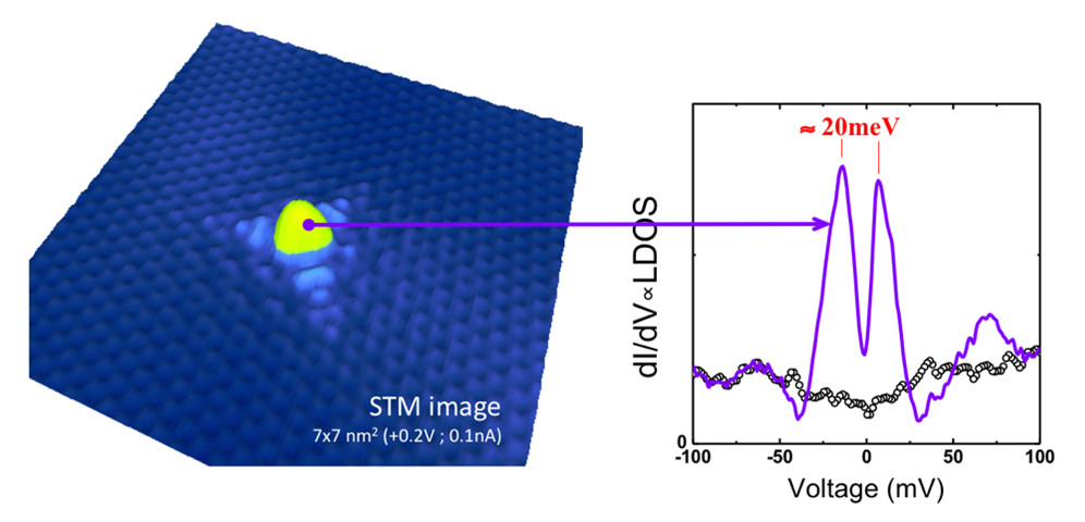
Isolated hydrogen atoms absorbed on graphene are predicted to induce magnetic moments. Here we demonstrate, by using STM complemented by first-principles calculations, that the adsorption of a single H atom on graphene induces a magnetic moment characterized by a 20 meV spin-split state at the Fermi energy. By using the STM tip to manipulate H atoms with atomic precision, it is possible to tailor the magnetism of selected graphene regions.
Collaborations :
Universidad Autonoma de Madrid
Publications :
Atomic-scale control of graphene magnetism by using hydrogen atoms, H. Gonzalez-Herrero, J.M. Gomez-Rodriguez, P. Mallet, M. Moaied, J.J. Palacios, C. Salgado, M.M. Ugeda, J.-Y. Veuillen, F. Yndurain, and I. Brihuega, Science 352, 437 (2016)
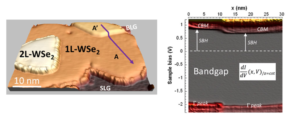
We performed STM/STS measurements to map the band onsets and the electronic bandgap of 2D semi-conducting TMDs such as WSe2 or MoSe2 deposited on Gr/SiC by mechanical exfoliation or MBE. We analyzed how these electronic properties are tuned by the substrate and by static disorder such as step edges, atomic scale defects, charged impurities, and boundaries.
Collaborations :
LNCMI Grenoble
SPINTEC Grenoble
Publications :
Scanning tunneling spectroscopy of van der Waals graphene/semiconductor interfaces: absence of Fermi level pinning, T. Le Quang, V. Cherkez, K. Nogajewski, M. Potemski, M.T. Dau, M. Jamet, P. Mallet, and J.-Y. Veuillen, 2D Materials 4, 035019 (2017)
Band-bending induced by charged defects and edges of atomically thin transition metal dichalcogenide films, T. Le Quang, K. Nogajewski, M. Potemski, M.T. Dau, M. Jamet, P. Mallet, and J.-Y. Veuillen, 2D Materials 5, 035034 (2018)
Benjamin Sacépé, Hermann Sellier
Alexis Coissard, Corentin Deprez, Marco Guerra, Hadrien Vignaud
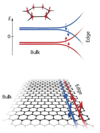
We unveiled a new interaction-induced topological phase in the zero-th Landau level of graphene. This phase is insulating in the bulk and exhibits a pair of spin-filtered, helical edge channels. It emerges under moderate perpendicular magnetic field when graphene is placed in proximity to a high-k dielectric substrate. In this work we demonstrate a remarkably robust quantum spin Hall effect that withstands up to 110 K over micron-long distances, which opens a new avenue for spintronics and topological superconductivity. More information
Publications :
Helical quantum Hall phase in graphene on SrTiO3, L. Veyrat, C. Déprez, A. Coissard, X. Li, F. Gay, K. Watanabe, T. Taniguchi, Z. V. Han, B. A. Piot, H. Sellier, and B. Sacépé, Science 367, 781 (2020)
Fundings :
ERC grant QUEST (2015-2020)
![]()
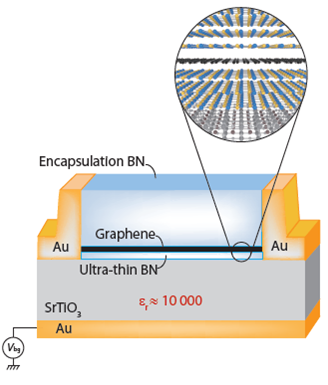
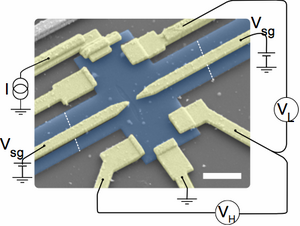
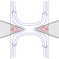
The absence of energy gap in graphene at zero magnetic field makes the fabrication of nanostructures difficult using metallic surface gates. In large magnetic fields however, the formation of Landau levels creates gaps in the spectrum, and the conducting edge channels follow the electrostatic potential of the gates. In this regime, quantum point contacts can be realized to control the number of channels transmitted through the device. The graphene flake can also be encapsulated between two boro-nitride flakes to boost its electron mobility. In such an heterostructure, the four-fold degeneracy of the Landau levels is lifted, and the fractional quantum Hall effect has been observed. Thanks to this unprecedented graphene quality, we achieved a precise control of the transmitted current through a quantum point contact, and more complex devices can now be studied, such as quantum Hall interferometers. More information
Publications :
Tunable transmission of quantum Hall edge channels with full degeneracy lifting in split-gated graphene devices, K. Zimmermann, A. Jordan, F. Gay, K. Watanabe, T. Taniguchi, Z. Han, V. Bouchiat, H. Sellier, and B. Sacépé, Nature Communications 8, 14983 (2017)
Low-magnetic-field regime of a gate-defined constriction in high-mobility graphene, L. Veyrat, A. Jordan, K. Zimmermann, F. Gay, K. Watanabe, T. Taniguchi, H. Sellier, and B. Sacépé, Nano Letters 19, 635 (2019)
Fundings :
ERC grant QUEST (2015-2020)
![]()
Hermann Sellier, Alexandre Assouline, Benjamin Sacépé, C. Bäuerle, S. Florens
The QuNES team’s research on Sound-driven 2D quantum circuits (S2D) brings together NEEL experts in 2D van der Waals materials (A. Assouline, B. Sacépé), surface acoustic wave-mediated single-electron transport (H. Sellier, C. Bäuerle), and theory of quantum circuits (S. Florens).
The S2D project aims to demonstrate a new platform for flying-electron qubits based on surface acoustic wave (SAW) driven single-electron transport in bilayer graphene.
Current solid-state qubits rely on localized systems, while photonic qubits, although propagating, cannot be dynamically controlled in flight. Flying electrons provide a powerful alternative : their propagation speed enables on-flight manipulation via electrical potentials, and Coulomb force gives a straightforward path to deterministic entanglement. Previous SAW-based experiments realized at NEEL in GaAs achieved 99.75 % transfer fidelity and controlled two-electron interactions, but dopant-induced excitations limit quantum coherence during propagation [1,2,3,4].
 |
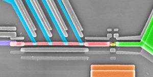
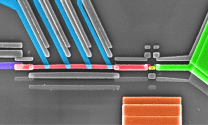
Scanning electron microscope image of a SAW device showing the metallic surface gates (light grey); taken from Ref [4]. The electron source (S1) consists of a quantum dot (shown in the top-left inset) coupled to a quantum point contact for charge sensing. The plunger gate (yellow) is used to inject an electron into a single SAW minimum. The Y-junction at the end of the central channel (see bottom inset) enables partitioning of the electron. Scale bars, 2 μm (main); 200 nm (insets). |
Graphene-based platforms, being dopant-free, allows ground-state preparation of propagating electrons. Moreover, high visiblity quantum interference has already been demonstrated in graphene mesoscopic circuits [5,6]. Single electron channels will be created in bilayer graphene, thanks to its electric-field-tunable bandgap. We will combine SAW-driven transport with bilayer graphene devices to implement real-time control of single electrons during flight and single-shot detection ; realizing the full potential of electron quantum optics.
 |
Bilayer graphene encapsulated in hBN dielectrics, equipped with graphite gates and a bottom graphene gate. The thin graphene gate is used to minimize screening of the SAW potential generated in the LiNbO3 substrate. |
[1] S. Takada et al., Sound-driven single-electron transfer in a circuit of coupled quantum rails, Nat. Commun. 10, 4557 (2019)
[2] J. Wang et al., Generation of a Single-Cycle Acoustic Pulse: A Scalable Solution for Transport in Single-Electron Circuits, Phys. Rev. X 12, 031035 (2022)
[3] J. Wang et al., Coulomb-mediated antibunching of an electron pair surfing on sound, Nat. Nanotechnol. 18, 721 (2023)
[4] J. Shaju et al., Evidence of Coulomb liquid phase in few-electron droplets, Nature 642, 928 (2025)
[5] C. Déprez et al., A tunable Fabry–Pérot quantum Hall interferometer in graphene, Nat. Nanotechnol. 16, 555 (2021)
[6] A. Assouline et al., Emission and coherent control of Levitons in graphene, Science 382, 1260 (2023)
Clemens Winkelmann, Hervé Courtois
Danial Majidi, Efe Gumus
Thermal transport in quantum devices is an interesting and yet vastly unexplored topic of research. We carried out thermal transport measurements through a single electron transistor (SET) where theory predicts a violation of some fundamental laws of physics. A thermal gradient is applied across the SET by cooling or heating the source (left) with a biased NIS junction while the drain (right) is thermalized to bath temperature. By measuring the temperature of the source as a function of the applied gate voltage using another NIS junction, we observed a periodic modulation of the heat conductance through the SET that shows a strong deviation from the usual Wiedemann-Franz law relating the charge and heat conductances.
Publications :
Thermal Conductance of a Single-Electron Transistor, B. Dutta, J. T. Peltonen, D. S. Antonenko, M. Meschke, M. A. Skvortsov, B. Kubala, J. König, C. B. Winkelmann, H. Courtois, and J. P. Pekola, Phys. Rev. Lett. 119, 077701 (2017)
Fundings :
Nanosciences Foundation Chair of Excellence of J. P. Pekola
LANEF PhD fellowship of Efe Gumus
Marie Curie ITN project QuESTech
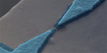
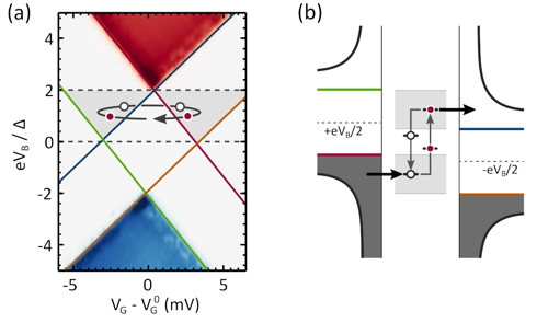
Electron transport through quantum dots coupled to superconducting leads shows a sharp conductance onset when a QD orbital level crosses one of the superconducting coherence peaks. Using individual gold nanoparticles connected to electromigrated aluminum leads, we showed that the hybridization of the QD levels with the leads is strongly enhanced by the divergent density of states at the superconducting gap edge. This result highlights the importance of cotunneling effects in spectroscopies with superconducting probes. In a regime where current is transported through a single level and driven by an ac gate voltage, we demonstrated single-electron-turnstile operation with a very narrow energy distribution and a higher immunity to nonequilibrium quasiparticles of the leads.
Publications :
Probing hybridization of a single energy level coupled to superconducting leads, D. M. T. van Zanten, F. Balestro, H. Courtois, and C. B. Winkelmann, Phys. Rev. B 92, 184501 (2015)
Single Quantum Level Electron Turnstile, D. M. T. van Zanten, D. M. Basko, I. M. Khaymovich, J. P. Pekola, H. Courtois, and C. B. Winkelmann, Phys. Rev. Lett. 116, 166801 (2016)
Fundings :
Nanosciences Foundation Chair of Excellence of J. P. Pekola
LANEF PhD fellowship of Alvaro Garcia-Corral
Marie Curie ITN project QuESTech
Hermann Sellier, Benjamin Sacépé
Diego Fossion
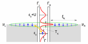
Gate-defined semiconductor quantum dots represent promising objects for quantum engineering. This project investigates the spatial extension of the many-body Kondo state that develops around these quantum dots at very low temperature. This Kondo cloud is a highly entangled state that could be used to coherently couple remote quantum dots distant by several microns. In this project, we employ scanning gate microscopy, a combined transport and scanning probe experiment, to measure the spatial extension of the Kondo cloud and to probe the Kondo-mediated coherent coupling between two quantum dots.
Collaborations :
Serge Florens (NEEL, team ThQC)
Louis Jansen, Marc Sanquer (CEA/INAC, Grenoble, France)
Dominique Mailly, Ulf Gennser (CNRS/C2N, Palaiseau, France)
Benoit Hackens, Vincent Bayot (UCL/IMCN, Louvain, Belgium)
Fundings :
ANR KONEX (2019-2023) KONdo-cloud EXtension around quantum dots
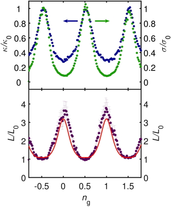
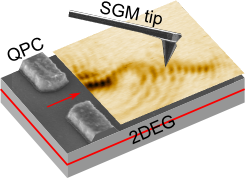
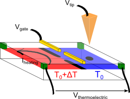
Electron-electron interactions in QPCs give rise to conductance anomalies below the first quantized plateau at 2e²/h, called 0.7 anomaly and zero-bias anomaly. Using scanning gate microscopy, we observed a repetitive splitting of the zero-bias anomaly when the tip approaches the QPC and tune the length of the quasi-1D channel, indicating the formation of a localized electron chain within the constriction, a sort of 1D Wigner crystal. Scanning gate interferometry close to the QPC revealed a phase shift of the electron interference in the bias range of the zero-bias anomaly, interpreted as a signature of localized states in the constriction with Kondo effect. We also introduced a new technique called Thermoelectric Scanning Gate Microscopy to probe quantum phenomena by measuring the thermoelectric voltage across the QPC instead of the conductance. This technique revealed a new phase shift in the tip-induced interference at very low conductance.
Publications :
Wigner and Kondo physics in Quantum Point Contacts revealed by Scanning Gate Microscopy, B. Brun, F. Martins, S. Faniel, B. Hackens, G. Bachelier, A. Cavanna, C. Ulysse, A. Ouerghi, U. Gennser, D. Mailly, S. Huant, V. Bayot, M. Sanquer, and H. Sellier, Nature Communications 5, 4290 (2014)
Electron Phase Shift at the Zero-Bias Anomaly of Quantum Point Contacts, B. Brun, F. Martins, S. Faniel, B. Hackens, A. Cavanna, C. Ulysse, A. Ouerghi, U. Gennser, D. Mailly, P. Simon, S. Huant, V. Bayot, M. Sanquer, and H. Sellier, Phys. Rev. Lett. 116, 136801 (2016)
Interference features in scanning gate conductance maps of quantum point contacts with disorder, K. Kolasinski, B. Szafran, B. Brun, and H. Sellier, Phys. Rev. B 94, 075301 (2016)
Thermoelectric scanning-gate interferometry on a quantum point contact, B. Brun, F. Martins, S. Faniel, A. Cavanna, C. Ulysse, A. Ouerghi, U. Gennser, D. Mailly, P. Simon, S. Huant, M. Sanquer, H. Sellier, V. Bayot, and B. Hackens, Phys. Rev. Applied 11, 034069 (2019)
Benjamin Sacépé
The interplay between disorder and superconductivity is a fundamental problem of condensed matter physics. Upon increasing disorder or magnetic field it is indeed possible to induce in a thin superconducting film a continuous quantum phase transition from a superconducting state to an insulating state led by the localization of electron pairs. Such zero-temperature transition, which involves Cooper pairs as charge carriers, provides a prototypical system to address the physics of the quantum localization of interacting bosons in disordered media. In this field we mainly focused our research on thin films of amorphous indium oxide, which exhibits a sharp superconductor-to-insulator transition. On the superconducting side of the transition, we have performed in close collaboration with C. Chapelier at INAC, the pioneering mK-STM spectroscopy study of the superconducting gap. Our work has demonstrated that Cooper pairs are not suppressed at the critical disorder but persist in insulators forming localized electron bound pairs. Beyond the critical disorder or critical magnetic field, the insulator that terminates superconductivity is attracting considerable interest due to mounting evidences that the charge carriers in it are electron pairs. In collaboration with D. Shahar from the Weizmann Institute of Science, we have performed magneto-transport studies on thin films. These experiments on insulators focus on the electron-phonon coupling in non-linear transport and on the possible many-body localization of charge carriers in this peculiar insulating state. More information
Position type: Stages Master-2 & Thèse
Contact: Sacépé Benjamin -
Hybridizing superconductivity with the quantum Hall (QH) effect has notable potential for designing circuits capable of inducing and manipulating non-Abelian states for topological quantum computation. A variety of QH states exhibits remarkable properties, as full spin polarization, helical phases with spin-momentum locking , fractionalization of charges into anyons quasiparticles, or a non-local nature and non-commutative braiding properties for non-Abelian anyons.
Position type: Stages Master-2 & Thèse
Contact: Assouline Alexandre - 0758572250
Anyons are quasiparticles that emerge in low-dimensional (d < 3) electronic systems. Their interest lies in their unconventional quantum statistics, neither bosonic nor fermionic, which allow manipulation of the system’s ground state by exchanging particle positions. This process, called braiding, is a route toward topological qubits with exceptionally low error rates. Moreover, the exploration of a new quantum statistics beyond the fermion–boson dichotomy is of considerable fundamental interest.
PhD grant available through ERC project: ANYONBOX
Person in charge: Benjamin SACEPE
Alexandre ASSOULINE
Personnel Chercheur - CNRS
alexandre.assouline [at] neel.cnrs.fr
Phone: 04 76 88 78 36
Office: D-306
Hervé COURTOIS
Personnel Chercheur - UGA
Herve.Courtois [at] neel.cnrs.fr
Phone: 04 76 88 11 51
Office: D-305
Benjamin SACEPE
Personnel Chercheur - CNRS
benjamin.sacepe [at] neel.cnrs.fr
Phone: 04 76 88 10 79
Office: D-307
Hermann SELLIER
Personnel Chercheur - UGA
hermann.sellier [at] neel.cnrs.fr
Phone: 04 76 88 10 86
Office: D-418
Jana AWAD
Personnel Chercheur - UGA
jana.awad [at] neel.cnrs.fr
Phone: 04 76 88 70 61
Office: D-318
Referent: Hervé COURTOIS
Nadjib BENCHABANE
Personnel Chercheur - CNRS
nadjib.benchabane [at] neel.cnrs.fr
Referent: Benjamin SACEPE
Johannes HOFER
Personnel Chercheur - UGA
johannes.hofer [at] neel.cnrs.fr
Phone: 04 76 88 12 24
Office: D-308
Referent: Clemens WINKELMANN
Nikolaos KOUTSOPOULOS
Personnel Technique - CNRS
nikolaos.koutsopoulos [at] neel.cnrs.fr
Office: D-313
Referent: Benjamin SACEPE
Mohammad MULLA-YUSUF
Personnel Chercheur - CNRS
mohammad.mulla-yusuf [at] neel.cnrs.fr
Referent: Alexandre ASSOULINE
Xiaoli PENG
Personnel Chercheur - CNRS
xiaoli.peng [at] neel.cnrs.fr
Referent: Benjamin SACEPE
Kalpajit ROY
Personnel Chercheur - CNRS
kalpajit.roy [at] neel.cnrs.fr
Referent: Benjamin SACEPE
Jashwanth SHAJU
Personnel Chercheur - CNRS
jashwanth.shaju [at] neel.cnrs.fr
Referent: Hermann SELLIER