- Accueil
- Institut Néel
- Équipes de recherche
- Pôles & Services techniques
- Travailler à l’institut
- Partenariats
- Actualités
- Agenda
- Annuaire
The Quan2m group gathers condensed matter physicists exploring quantum states hosted by two-dimensional materials (graphene and transition metal dichalcogenides for instance). We focus on quantum states involving different kinds of excitations, electronic, phononic or magnonic, possibly related to strong interaction effects, and seek ways to tune these interactions. This is done via, e.g., electromagnetic fields, mechanical deformations, the proximity to magnetic or superconducting materials, or by controlling structural parameters such as the twist angle between two stacked 2D materials.
The group’s research currently deals with four classes of effects, respectively relevant in (i) quantum optoelectronics, (ii) quantum engineering, (iii) optothermics and (iv) 2D ordering phenomena. We operate various equipments to probe these effects: low-temperature magnetotransport setups, optical spectroscopy measurement lines, and a comprehensive platform (2Dfab) for the fabrication of artificial 2D heterostacks. Besides, we have direct access to various growth, advanced nanocharacterization, and nanofabrication facilities.
Quantum optoelectronics
Quantum engineering
Optothermics
2D ordering phenomena
The variety of available low-dimensional systems gives access to a wealth of electronic properties, among which direct bandgap allows for optoelectronic applications. Interestingly, all low-dimensional materials we investigate exhibit optical phonons that couple to electrons and can be probed with Raman spectroscopy.
We investigate interlayer and intralayer excitons, free carriers in low-dimensional materials in a transistor configuration, excitonic interactions, defects as photon sources [1,2]. Photoluminescence and Raman spectroscopy along with electronic transport provide insights into the electronic structure and transitions at play in heterostructures. In addition, we take advantage of the possible functionalization of low-dimensional systems via pi-stacked molecules to explore phenomena such as charge or energy transfer as well as light-activated tunneling [3].
[1] S. Dubey et al., ACS Nano 11, 11206 (2017)
[2] G. Nayak et al., Phys. Rev. Materials 11, 114001 (2019)
[3] Y. Chen et al., Advanced Materials 31, 1902917 (2019).
Contact : laetitia.marty@neel.cnrs.fr
We couple two dimensional materials to confined electromagnetic fields in order to study interacting quantum systems in different regimes.
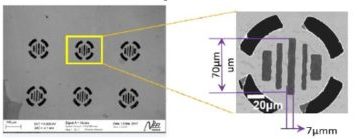
In superconducting circuits, working with microwave photons, we integrate graphene electronic transport channels and exploit their unique gate tunability. More specifically, we have recently demonstrated a gate tunable Josephson parametric amplifier that operates at the quantum limit [1]. The tunability of graphene Josephson junctions is also promising for the gate tunable superconducting Qubits we are currently developing.
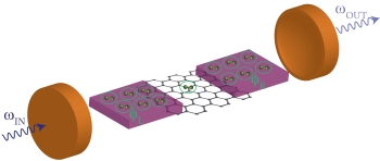
In the optical domain, we integrate 2D transition metal dichalcogenides (TMDC) within microcavities. We focus on the interaction between optical excitations (i.e. excitons), which is peculiar in TMDCs, in order to demonstrate non-classical sources of photons [2].
[1] G. Butseraen et al., Nat. Nanotechnol. 17, 1147 (2022)
[2] P. Stepanov et al., Phys. Rev. Lett. 126, 167401 (2021)
Contact: julien.renard@neel.cnrs.fr
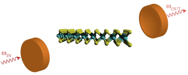
A monolayer transition metal dichalcogenides inserted in an optical microcavity
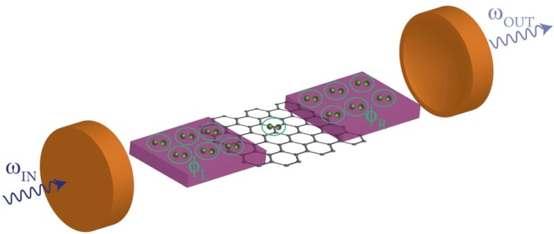
A graphene based Josephson junction can be inserted in a microwave cavity to allow gate tunability
One-atom thick membranes, which are surfaces with no bulk exhibit unusual thermal and mechanical properties. In particular, graphene exhibits very high thermal conductivity and thermal regimes not fully elucidated yet.
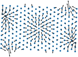
We use optical techniques, in particular Raman spectroscopy, for thermal measurements of 2D membranes. We recently implemented a two-laser approach using one laser as the heater and the other as the local temperature probe. This allows imaging the spatial temperature distribution and thereby directly determining heat fluxes, which we analyse with models beyond the Fourier law [1]. This opens new perspectives on thermal transport at the nanoscale.
[1] P. Singh et al., PhD manuscript, UGA (2022)
In two-dimensional systems, a multitude of commensurate and incommensurate phases, topological phase transitions, highly degenerate ground states, etc, can occur. We explore such phases related to structural (e.g. moiré patterns), spin (e.g. magnetically-ordered phases) and charge (e.g. charge density waves, superconducting states) degrees of freedom, in presence of classical and quantum kinds of interactions.
We investigate these (dis)order phenomena in epitaxial two-dimensional systems (graphene, transition metal dichalcogenides) forming various kinds of commensurate and incommensurate super-orders ; and in exfoliated metallic transition metal dichalcogenides, some of which are prone to electronic instabilities mediated by interactions with phonons (TaS2, TaSe2) and others to magnetic ordering up to room temperature (CrTe2). Thickness-dependent order/disorder is probed at the atomic scale with scanning tunneling microscopy, with high-resolution synchrotron X-ray diffraction, and with the help of optical probes, Raman spectroscopy and magneto-optical Kerr effect magnetometry at variable temperatures and with spatial resolution.
[1] A. Purbawati, S. Sarkar et al. ACS Appl. Elec. Mater. ASAP article
[2] S. Layek et al.,. Carbon, 201, 667 (2023).
[3] S. Lisi et al. Phys. Rev. Lett. 129, 096101 (2022)
[4] A. Purbawati et al. ACS Appl. Mater. Interf. 12, 30702 (2020)
Contact: johann.coraux@neel.cnrs.fr
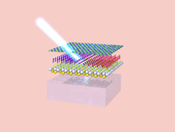
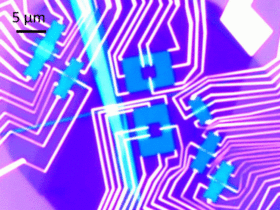
Van der Waals heterostructures, tailor-made crystals obtained by stacking 2D materials, open a wide range of new functions in condensed matter. Fine tuning of the different interactions at play in 2D heterostructures is achieved with the use of few layer graphene electrostatic gates, with the controlled mismatch angle between layers and other nanofabrication techniques compatible with 2D materials.
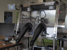
The 2Dfab platform is operated in collaboration with the QNES team, and with support from the Nanofab and Experimental Engineering technical groups of the lab. It gathers state-of-the-art, in-house-developed manipulation tools including micro-transfer stages for dry stamping 2D materials one of which is operated within our Ar glove-box. Further processing can be performed like annealing, or surface treatments in a clean chemistry room, while device fabrication is performed at the Nanofab facility.
[1] D. Dufeu, et al., Highlights – Institut Néel, 20 (2016).
[2] L. Marty, et al., Nanosciences Fondation Graphene Highlights, 25 (2013).
Position type: Stages Master-2 & Thèse
Contact: Laetitia Marty - | Nedjma Bendiab -
This internship aims at using carotenoid molecules asociated to low dimension materials for an efficient collection of light-generated electrons.
Position type: Stages Master-2 & Thèse
Contact: Coraux / Johann - +33 4 7688 1289
The internship is focused on charge density waves —macroscopic quantum states consisting in a coherent spatial modulation of the charge in a crystal— and how they can experience a proximity effect, i.e. live in a crystal that does not naturally develop such quantum phases but can host them when put in contact to another crystal. This effect will be studied in two-dimensional crystals, and will be scrutinized using cryogenic optical spectroscopy and electron diffraction.
Position type: Post-doc
Contact: Jérémie Viennot - | Julien Renard -
This project aims at developing a microwave-optical quantum interface to be used as a key element in future quantum technologies. Such an interface will permit long-distance transfer of microwave quantum information and enable optically-mediated entanglement of distant microwave qubits.
Person in charge: Julien RENARD
Permanents
Students & Post-docs & CDD
Nedjma BENDIAB
Personnel Chercheur - UGA
nedjma.bendiab [at] neel.cnrs.fr
Phone: 04 76 88 79 06
Office: D-204
Johann CORAUX
Personnel Chercheur - CNRS
johann.coraux [at] neel.cnrs.fr
Phone: 04 76 88 12 89
Office: K-205
Laurence MAGAUD
Personnel Chercheur - CNRS
Laurence.Magaud [at] neel.cnrs.fr
Phone: 04 76 88 74 63
Office: C3-207
Pierre MALLET
Personnel Chercheur - CNRS
Pierre.Mallet [at] neel.cnrs.fr
Phone: 04 76 88 74 52
Office: D-404
Laëtitia MARTY
Personnel Chercheur - CNRS
Laetitia.Marty [at] neel.cnrs.fr
Phone: 04 56 38 70 42
Office: D-203
Julien RENARD
Personnel Chercheur - CNRS
julien.renard [at] neel.cnrs.fr
Phone: 04 56 38 71 76
Office: Z-219
Jean-Yves VEUILLEN
Personnel Chercheur - CNRS
Jean-Yves.Veuillen [at] neel.cnrs.fr
Phone: 04 76 88 74 61
Office: D-414
Christos ANASTASSIADES
Personnel Chercheur - CNRS
christos.anastassiades [at] neel.cnrs.fr
Phone: 04 76 88 74 28
Office: D-216
Referent: Julien RENARD
Aloïs ARRIGHI
Personnel Chercheur - CNRS
alois.arrighi [at] neel.cnrs.fr
Referent: Laëtitia MARTY
Carlos Rodolfo BOMFIM LOPES SOUZA
Personnel Chercheur - G-INP
carlos.souza [at] neel.cnrs.fr
Referent: Laëtitia MARTY
Adan CASTILLO-GUERRERO
Personnel Chercheur - UGA
adan.castillo-guerrero [at] neel.cnrs.fr
Phone: 04 76 88 74 28
Office: D-216
Referent: Julien RENARD
Pranjal KAPOOR
Personnel Chercheur - UGA
pranjal.kapoor [at] neel.cnrs.fr
Phone: 04 76 88 74 28
Office: D-216
Referent: Julien RENARD
Seong-Yeon LEE
Personnel Chercheur - CNRS
seong-yeon.lee [at] neel.cnrs.fr
Office: Z-215
Referent: Julien RENARD
Tristan RICCARDI
Personnel Chercheur - CNRS
tristan.riccardi [at] neel.cnrs.fr
Referent: Johann CORAUX
Mostafa SALEH
Personnel Chercheur - CNRS
mostafa.saleh [at] neel.cnrs.fr
Referent: Johann CORAUX
Giuseppe BUCCOLIERO
Personnel Chercheur - CEA
giuseppe.buccoliero [at] neel.cnrs.fr
Phone: 04 76 88 79 14
Office: K-207
Referent: Johann CORAUX
Ruben-Alejandro ORTIZ-FRANCISCO
Personnel Chercheur - ESRF
ruben-alejandro.ortiz-francisco [at] neel.cnrs.fr
Referent: Johann CORAUX