- Home
- Institut Néel
- Research teams
- Technical Groups & Services
- Work at the Institut
- Partnerships


Since 2010 I work at the Neel Institute in Grenoble.
The complete list of my publications, including citation metrics, can be found here using Publons or here using Google citations search engines.
I am interested in the structure properties relation of semiconducting nanowires (NWs) using transmission electron microscopy (TEM), optical spectroscopy and electron transport, as well as in-situ TEM experiments. The goal of my research is to develop methods to combine various characterization methods (optical and electrical) with transmission electron microscopy characterization on the same unique nanowire, and find what structural or electrical properties at the sub-nm scale determine the macroscopically measured optical and electrical properties of the nano-structure. For electrical and electro-optical characterization contacts have to be applied to the nanowire, that can also be used to bias the nanowire device in-situ in the transmission electron microscope. Observing the reaction of a device to an electrical signal with nm scale resolution is a very exiting opportunity to learn more on the device characteristics/reactions, and will allow ultimately to correlate the presence of a single impurity atom observed in TEM with electrical spectroscopy of this same single atom in a single dopant device.
I am interested in the structure properties relation of semiconducting nanowires (NWs) using transmission electron microscopy (TEM), optical spectroscopy and electron transport. Moreover, I’m interested to use electrical in-situ biasing of objects such as nanowires to learn more about the electrical properties at nm length scales. The goal of my research is to develop methods to combine various characterization methods (optical and electrical) with transmission electron microscopy characterization on the same unique nanowire, and find what structural or electrical properties at the sub-nm scale determine the macroscopically measured optical and electrical properties of the nano-structure. For electrical and electro-optical characterization contacts have to be applied to the nanowire, that can also be used to bias the nanowire device in-situ in the transmission electron microscope. Observing the reaction of a device to an electrical signal with nm scale resolution is a very exiting opportunity to learn more on the device characteristics/reactions, and will allow ultimately to correlate the presence of a single impurity atom observed in TEM with electrical spectroscopy of this same single atom in a single dopant device.
To realize these type of NW devices we fabricate nitride membranes at the Nanofab cleanroom in Neel, that are compatible with TEM and cleanroom fabrication procedures such as optical and electron beam lithography.
My research can be divided in two parts. (i) TEM characterization of semiconducting NWs to observe quantum dot insertions and other NW qualities such as cristallinity, size, strain etc. Furthermore (ii) I develop electrical in-situ experiments, working both on propagation of metals in the NW to improve the contact quality and control the size of the semiconducting region between the contacts with nm precision. Again with the idea to correlate the structural properties of the object with the electrical properties. Furthermore I use off-axis electron holography in combination with in-situ biasing with the aim to quantitatively measure doping concentration, surface charges and internal polarization fields in NWs. I have obtained promising first results looking at the depletion width at a Schotkey contact on a ZnO NW.
I gave a seminar for the Institut de Minéralogie, de Physique des Matériaux et de Cosmochimie (Sorbonne Université, Paris) about In-situ transmission electron microscopy biasing and heating experiments of semiconducting nanowires for correlated studies and electrical contact formation. Here you can see the recorded presentation (unfortunately, some of the movies and images are not displayed correctly, the relevant references are provided to see the video in decent quality).
Welcome to Bruno Cesar da Silva, who is starting his postdoc with me in the framework of the e-See ERC!
I gave a nanotalk for Denssolutions about our work on in-situ biasing using their six contacts Lightning holder, it was fun. Here you can see the recorded presentation, which gives a good overview of my research.
Received the bronze medal of CNRS. A very big honour! Here you can see the video in honour of this event, nicely illustrating my research (in the french language).
Welcome to Zahra Sadre Momtaz, who is starting her postdoc with me in the framework of the e-See ERC!
Obtained an ERC starting grant to develop cryogenic in-situ TEM to detect a single charge in a device using TEM. I will have open postdoctoral and PhD positions.
Welcome to Meije Verbeek, my lovely new daughter!
Welcome to Maria Spies and Minh Anh Luong, who are both starting their PhD.
Obtained an Amadeus PCH grant to facilitate traveling with the collaborating group of Alois Lugstein in Vienna!
Welcome to Akhil Ajay, starting his PhD with Eva Monroy and me.
Doing in-situ high speed experiments in Ernst Ruska Center Julich, with Martial, Vadim, Khalil, Henning and Martin.
Welcome to my son Sam Verbeek, just born!
Welcome to Khalil Elhajraoui who is starting his PhD!
Start of my young researcher ANR (Agence National de la Recherche) project: Correlation of transmission electron microscopy (TEM) with optical and electrical characterization of the same unique nano-object (COSMOS).
Obtained a position as permanent researcher at Institut Neel, CNRS.
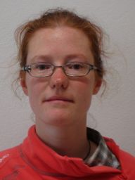
Dr. Martien den Hertog (female), CNRS researcher, obtained her MSc degree in Chemistry and Physics from the University of Utrecht (NL) in 2005 and PhD in 2009 from University Joseph Fourier in Grenoble on transmission electron microscopy of nanostructures. Since 2010 she is working as a junior researcher at the Institut Neel to develop methods to study nano-object based devices by correlation of electrical and structural properties and electrical in-situ TEM experiments. She has been coordinator of a French young researcher project (ANR project COSMOS) and has received and ERC starting grant e-See that started in Oktober 2018.
Since 2018 I enjoy an ERC starting grant to develop cryogenic in-situ TEM with the final goal to detect a single charge in a device using TEM based methods. I’m most greatful to the ERC for giving me the opportunity to carry out such fascinating research!
I have strong collaborations with the NPSC group, as well as the LEMMA group on TEM inside IRIG/CEA-Grenoble at the NanoCharacterization Platform (PFNC). I also collaborate with the SINAPS team.
Outside Grenoble I have a collaborations with researchers at CEMES Toulouse, the Technical University of Vienna, Antwerpen University and Bremen University.

Logo du CEA
Department: PLUM
Team: Materials, Radiations, Structure (MRS)
Status: Personnel Chercheur
Structure: CNRS
Position: Permanent
Email: martien.den-hertog@neel.cnrs.fr
Phone: 04 76 88 10 45
Office: F-313
