- Home
- Institut Néel
- Research teams
- Technical Groups & Services
- Work at the Institut
- Partnerships
The EpiCM technological group develops and optimizes original experimental set-ups operating mainly under vacuum and ultra-high vacuum as well as processes for growing innovative nano-materials. The diversity of produced materials is wide by their types and properties (semiconductors, metals, magnetic materials, superconductors, oxides and functionalized materials) as well as by their forms (thin layers, nano-objects and two-dimensional). EpiCM member’s skills in instrumental development, materials synthesis and related characterizations are provided to researchers with high quality interaction. Furthermore, the EpiCM group is also involved in some collaborative research projects with other public or private research laboratories and institutes.
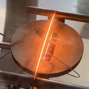
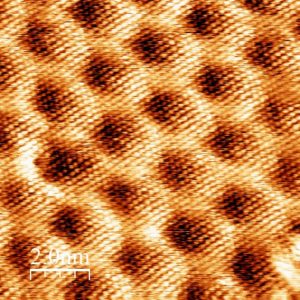
Carbon nanotubes deposition by CVD STM image of graphene grown under UHV
The Epitaxy and thin layer (EpiCM) technological group operates and develops several growth set-ups: Molecular beam epitaxy (MBE), magnetron sputtering (PVD), pulsed laser deposition (PLD) and chemical vapor deposition (CVD) that are dedicated to the growth of epitaxial thin films of semiconductors, oxides and metals. The group collaborates with several research teams from Institut Néel and provides technical support to any user from the laboratory with a specific need in material development. The group is also largely involved in the design and supervision of new experimental environments (sputtering deposition reactor for metals and oxides multilayers, new multi technique chambers for epitaxy, clean rooms) as well as in the upgrade of existing reaction chambers. It contributes to the emergence of new research fields such as low dimensional object synthesis (quantum dots, semiconducting or magnetic nanowires, epitaxial graphene or transition metal dichalcogenide monolayers on metal, carbon nanotubes and diamond thin films). Furthermore, the EpiCM group is involved in high quality epitaxial thin film growth and characterization measurements in collaboration with research teams and other technological groups of Institut Néel. Thanks to its expertise in growth and instrumental development, the group manages material growth workpackages for several projects with researchers from other laboratories and institutes. Members of the EpiCM group are also strongly involved in the laboratory collective tasks such as trainings and safety and prevention.
… coming soon …
Cette page est vide.
Cette page est vide.
Cette page est vide.
… coming soon …
Cette page est vide.
Cette page est vide.
Cette page est vide.
Cette page est vide.
Position type: Bachelor and Master 1 internships
Contact: ABBASSI Latifa - +33 (0)4 76 88 79 31 | CLAUDEL Arnaud - +33 (0)4 76 88 78 83
La silanisation est un procédé de traitement de surface permettant de modifier l’hydrophilie ou l’hydrophobie des substrats. Cette fonctionnalisation est cruciale pour préparer des surfaces photovoltaïques à des applications avancées, telles que le transfert de matériaux 2D (par exemple le graphène) pour remplacer l’ITO. Le laboratoire dispose d’un bâti de silanisation Diener, installé dans la salle propre de nanochimie, permettant un contrôle précis des paramètres de traitement.
Position type: Master 2 internships and theses
Contact: Arnaud CLAUDEL - +33 (0)4 76 88 78 83 | Latifa ABBASSI - +33 (0)4 76 88 79 31
La production actuelle de cellules photovoltaïques (PV) utilise une quantité importante de couches d’oxyde conducteur transparent (TCO) à base d’indium. Dans un contexte prévisible de pénurie en indium, une piste possible consiste à remplacer le TCO à base d’indium par du graphène comme couche conductrice transparente. Le graphène, en plus d’être composé de carbone, un élément abondant sur Terre et donc non critique, peut présenter une excellente transparence optique et de très bonnes propriétés électriques.
Les principaux objectifs de ce stage seront de développer et optimiser des procédés de report de couches de graphène par voie humide et sèche sur des précurseurs de cellules PV, en utilisant des techniques de traitement et de fonctionnalisation de surface.
L’Institut Néel dispose d’un équipement dédié à l’élaboration de graphène et d’environnements adaptés (salles de chimie, salles blanches) pour réaliser à la fois le report et les caractérisations de ce matériau sur des substrats « hôtes ».
Person in charge: Arnaud CLAUDEL
Permanents
Latifa ABBASSI
Personnel Technique - CNRS
latifa.abbassi [at] neel.cnrs.fr
Phone: 04 76 88 79 31
Office: Z-125
David BARRAL
Personnel Technique - CNRS
David.Barral [at] neel.cnrs.fr
Phone: 04 76 88 79 30
Office: D-107
Arnaud CLAUDEL
Personnel Technique - CNRS
arnaud.claudel [at] neel.cnrs.fr
Phone: 04 76 88 78 83
Office: D-411
Philippe DAVID
Personnel Technique - CNRS
Philippe.David [at] neel.cnrs.fr
Phone: 04 76 88 74 39
Office: D-210
Stéphanie GARAUDEE
Personnel Technique - CNRS
Stephanie.Garaudee [at] neel.cnrs.fr
Phone: 04 76 88 74 19
Office: F-213
Pierre GASNER
Personnel Technique - CNRS
pierre.gasner [at] neel.cnrs.fr
Phone: 04 76 88 79 67
Office: E-217b
Pierre GIROUX
Personnel Technique - CNRS
Pierre.Giroux [at] neel.cnrs.fr
Phone: 04 76 88 79 23
Office: D-415
Gaël MOIROUX
Personnel Technique - CNRS
gael.moiroux [at] neel.cnrs.fr
Phone: 04 76 88 79 73
Office: E-217b
Julien BAYON
Personnel Technique - CNRS
julien.bayon [at] neel.cnrs.fr
Referent: Yann GENUIST
Noé BONINO
Personnel Technique - CNRS
noe.bonino [at] neel.cnrs.fr
Phone: 04 76 88 79 36
Office: E-209
Referent: Gaël MOIROUX
Oscar BRAND
Personnel Technique - CNRS
oscar.brand [at] neel.cnrs.fr
Referent: Arnaud CLAUDEL
Antoine DOMENECH
Personnel Chercheur - CNRS
antoine.domenech [at] neel.cnrs.fr
Phone: 04 56 38 71 80
Office: D-413
Referent: Arnaud CLAUDEL