- Home
- Institut Néel
- Research teams
- Technical Groups & Services
- Work at the Institut
- Partnerships

I am a CNRS researcher at the Néel Institute, and member of the SC2G team.
The experiments I am developping aim to access the optical and electricals properties of wide bandgap semiconductor materials at the nanoscale.
The originality of this research involves exploiting and combining light-matter and electron-matter interactions. The objective of my research aims to understand the physics that currently limit the efficiency of key devices such as power transistors and light-emitting diodes. In particular, I am continuously striving to develop novel experiments that accurately measure the impact of defects on various optoelectronic devices efficiency. Given the nanometric dimensions of the objects I investigate, such as nanowires, point defects and dislocations, I am bound by the diffraction limit of visible light. That’s why, in order to achieve the best possible spatial resolution, I often make use of an accelerated electron beam.
The foundation of most of my experiments is the physical phenomenon that occurs when the electron beam interacts with matter and generates a significant amount of free carriers, namely electrons and holes. Once electron/hole pairs are generated in a device, they possess three potential outcomes:
For each of these processes, I develop adapted experimental setups that you can find in the Experimental setups section.
After more than 30 years of development, light-emitting diodes (LEDs) based on nitrides such as gallium nitride are widely used for general lighting. Microdisplays for virtual or augmented reality are now a new area of application. These miniaturised display technologies require pixel sizes of less than 10 µm, known as micro-LEDs (μLEDs). To obtain a µLED, it is necessary to etch the material, which creates defects. By breaking the crystal structure, etching creates so-called “dangling” bonds. These are then available to bond to any atom, creating impurities. The smaller the LED, the more these defects affect the behaviour of the device as surface effects become important. Passivation technologies exist to limit their influence. This involves depositing a protective layer on the etch flank to occupy the dangling bonds. However, the small pixel size, measurement artefacts and wide variety of passivation methods make it difficult to compare efficiency gains between different technological solutions. Studying the influence of the surface on the efficiency of μLEDs requires a combination of spatial resolution of a few tens of nanometres (nm, 10-9 m) and temporal resolution of a few tens of picoseconds (ps, 10-12 s).

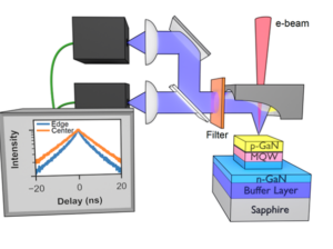
My aim is to quantify the influence of surface defects on the efficiency of micro-LEDs based on element III nitrides. This work is carried out in collaboration with the CEA-LETI. The originality of this work lies in the fact that I have developed a non-destructive method to measure the influence of surface recombination with a spatial resolution of the order of 50 nm and a temporal resolution of the order of 50 ps. This method is all the more relevant because it uses a conventional scanning electron microscope and cleverly exploits the specific features of electron-light-matter interactions (Figure 1). Measuring the local efficiency of micro-LEDs after the initial stages of cleanroom fabrication opens up a number of new perspectives. First, it eliminates the need to run the entire costly technology process to estimate the impact of surface passivation. Secondly, it provides a metric that allows effective comparison of different passivation techniques.
References
Surface Recombinations in III-Nitride Micro-LEDs Probed by Photon-Correlation Cathodoluminescence. Sylvain Finot, Corentin Le Maoult, Etienne Gheeraert, David Vaufrey, and Gwénolé Jacopin, ACS Photonics, publié le 07 décembre 2021.
DOI: 10.1021/acsphotonics.1c01339
Under construction
Under construction
Under construction
Under construction
Under construction
Department: PLUM
Team: Wide bandgap semiconductors (SC2G)
Status: Personnel Chercheur
Structure: CNRS
Position: Permanent
Email: gwenole.jacopin@neel.cnrs.fr
Phone: 04 76 88 11 83
Office: D-312
