- Home
- Institut Néel
- Research teams
- Technical Groups & Services
- Work at the Institut
- Partnerships

 Sébastien PAIRIS – Material Characterization Dip. Ing. Fr
Research Engineer at CNRS / Institut Néel , Lecturer at Université Grenoble Alpes (UGA) and Training manager of the “Microscopy and Microanalysis course” (CNRS/Formation Entreprises)
Lecturer at Université Grenoble Alpes (UGA)
Training Manager of “Microscopy and Microanalysis Courses”
The Ultima CBED program is dedicated to Convergent-Beam Electron Diffraction patterns obtained in transmission electron microscopy in two-beam conditions. The software was developed with Visual Basic 5.0 Language by S. PAIRIS from the CNRS – Laboratoire de Cristallographie.
The code and the application have been deposited at the agency for software protection (APP) in October 2005 with serial number IDDN.FR.001.400043.000.D.P.2005.000.31235.
The licence of Ultima CBED is a CeCILL type; it’s a freeware program.
Ultima CBED software is used to determine the foil thickness of crystallized specimens by the Kelly’s method [1]. After the input of instrumental and cristallographic parameters (High Voltage, hkl interplanar spacing of the diffracted beam, extinction distance g, if possible the anomalous absorption distance) and of the experimental parameters (diameter of the disk, distance between diffracted and transmitted disks, distance between two symmetric fringes in the diffracted disk), the program calculates the deviation parameters Si. Using the display index ni, Ultima CBED also calcules X and Y as definited previously. The thickness is obtained from a linear regression. It is then used to simulate the rocking-curve and the diffraction pattern corresponding to the conditions given by the user and to the same thickness. The convergence angle and the experimental camera length are calculated too.
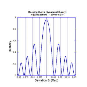
In a second step, it’s possible to simulate CBED pattern in two-beam conditions by enterring the thickness, the convergence of the beam, the interplanar distance of the diffracted beam and the extinction distance. The pattern can be simulated either in kinematical or dynamical approach. The rocking – curve is plotted.
Two – beam orientation on Silicon; Reflection g = (220) ; d = 1,92 Å ; Simulation with dynamical theory
Thickness = 265 nm ; 300kV – 2a= 0,23°
Experimental Extinction distance computed with fringes: 103,47 nm
Theorical Extinction distance of the diffracted beam (220) : 103,2 nm
|
|
 |
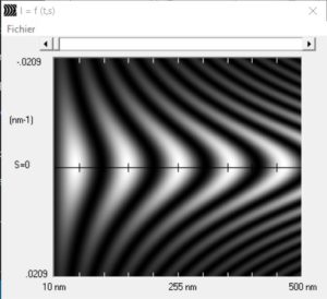
Finally, Ultima CBED enables to simulate (with kinematical or dynamical theory) intensity maps as a function of the thickness and of the deviation parameters Si. A cursor in a scrollbar can be moved in order to select the thickness. When the cursor is moved on the map, the modulations of the intensity (rocking – curve) and the simulated pattern are plotted on-line. The linear regressions and the rocking – curves can be saved in text or picture format. The patterns and the maps can be saved in picture format.
Two – beam orientation on Silicon; Reflection g = (220) ; d = 1,92 Å ; Simulation with dynamical theory
Thickness = from 10nm to 500nm ; 300kV – 2a= 0,23°
Theorical Extinction distance of the diffracted beam (220) : 103,2 nm

[1] KELLY P.M., JOSTSONS A., BLAKE R.G., NAPIER J.G., « Determination of foil thickness by scanning transmission electron microscopy », Physica Status Solidi A, 1975
Member of microscopy network:
Member of materials network:
Department: MCBT
Status: Personnel Technique
Structure: CNRS
Position: Permanent
Email: Sebastien.Pairis@neel.cnrs.fr
Phone: 04 76 88 90 25
Office: F-213
